- 您现在的位置:买卖IC网 > PDF目录19403 > ADSP-BF514KSWZ-3 (Analog Devices Inc)IC DSP 16/32B 300MHZ LP 176LQFP PDF资料下载
参数资料
| 型号: | ADSP-BF514KSWZ-3 |
| 厂商: | Analog Devices Inc |
| 文件页数: | 5/68页 |
| 文件大小: | 0K |
| 描述: | IC DSP 16/32B 300MHZ LP 176LQFP |
| 标准包装: | 40 |
| 系列: | Blackfin® |
| 类型: | 定点 |
| 接口: | I²C,PPI,RSI,SPI,SPORT,UART/USART |
| 时钟速率: | 300MHz |
| 非易失内存: | 外部 |
| 芯片上RAM: | 116kB |
| 电压 - 输入/输出: | 1.8V,2.5V,3.3V |
| 电压 - 核心: | 1.30V |
| 工作温度: | 0°C ~ 70°C |
| 安装类型: | 表面贴装 |
| 封装/外壳: | 176-LQFP 裸露焊盘 |
| 供应商设备封装: | 176-LQFP-EP(24x24) |
| 包装: | 托盘 |
第1页第2页第3页第4页当前第5页第6页第7页第8页第9页第10页第11页第12页第13页第14页第15页第16页第17页第18页第19页第20页第21页第22页第23页第24页第25页第26页第27页第28页第29页第30页第31页第32页第33页第34页第35页第36页第37页第38页第39页第40页第41页第42页第43页第44页第45页第46页第47页第48页第49页第50页第51页第52页第53页第54页第55页第56页第57页第58页第59页第60页第61页第62页第63页第64页第65页第66页第67页第68页
ADSP-BF512/BF512F, BF514/BF514F, BF516/BF516F, BF518/BF518F
Rev. B
|
Page 13 of 68
|
January 2011
TNOM is the duration running at fCCLKNOM
TRED is the duration running at fCCLKRED
VOLTAGE REGULATION INTERFACE
The ADSP-BF51x processors require an external voltage regula-
tor to power the VDDINT domain. To reduce standby power
consumption in the hibernate state, the external voltage regula-
tor can be signaled through EXT_WAKE to remove power from
the processor core. The EXT_WAKE signal is high-true for
power-up and may be connected directly to the low-true shut
down input of many common regulators.
The Power Good (PG) input signal allows the processor to start
only after the internal voltage has reached a chosen level. In this
way, the startup time of the external regulator is detected after
hibernation. For a complete description of the PG functionality,
refer to the ADSP-BF51x Blackfin Processor Hardware Reference.
CLOCK SIGNALS
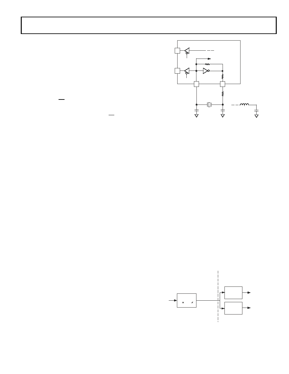
The ADSP-BF51x processors can be clocked by an external crys-
tal, a sine wave input, or a buffered, shaped clock derived from
an external clock oscillator.
If an external clock is used, it should be a TTL compatible signal
and must not be halted, changed, or operated below the speci-
fied frequency during normal operation. This signal is
connected to the processor CLKIN signal. When an external
clock is used, the XTAL pin/ball must be left unconnected.
Alternatively, because the processor includes an on-chip oscilla-
tor circuit, an external crystal may be used. For fundamental
frequency operation, use the circuit shown in Figure 4. A paral-
lel-resonant, fundamental frequency, microprocessor-grade
crystal is connected across the CLKIN and XTAL pins/balls. The
on-chip resistance between the CLKIN pin/ball and the XTAL
pin/ball is in the 500 kΩ range. Further parallel resistors are typ-
ically not recommended. The two capacitors and the series
resistor shown in Figure 4 fine tune phase and amplitude of the
sine frequency.
The capacitor and resistor values shown in Figure 4 are typical
values only. The capacitor values are dependent upon the crystal
manufacturers’ load capacitance recommendations and the PCB
physical layout. The resistor value depends on the drive level
specified by the crystal manufacturer. The user should verify the
customized values based on careful investigations on multiple
devices over temperature range.
A third-overtone crystal can be used for frequencies above 25
MHz. The circuit is then modified to ensure crystal operation
only at the third overtone, by adding a tuned inductor circuit as
shown in Figure 4. A design procedure for third-overtone oper-
ation is discussed in detail in application note (EE-168) Using
Third Overtone Crystals with the ADSP-218x DSP on the Analog
Devices website (www.analog.com)—use site search on
“EE-168.”
The CLKBUF signal is an output signal, which is a buffered ver-
sion of the input clock. This signal is particularly useful in
Ethernet applications to limit the number of required clock
sources in the system. In this type of application, a single
25 MHz or 50 MHz crystal may be applied directly to the pro-
cessor. The 25 MHz or 50 MHz output of CLKBUF can then be
connected to an external Ethernet MII or RMII PHY device.
The Blackfin core runs at a different clock rate than the on-chip
peripherals. As shown in Figure 5, the core clock (CCLK) and
system peripheral clock (SCLK) are derived from the input
clock (CLKIN) signal. An on-chip PLL is capable of multiplying
the CLKIN signal by a programmable 5× to 64× multiplication
factor (bounded by specified minimum and maximum VCO
frequencies). The default multiplier is 6×, but it can be modified
by a software instruction sequence.
On-the-fly frequency changes can be done simply by writing to
the PLL_DIV register. The maximum allowed CCLK and SCLK
rates depend on the applied voltages VDDINT, VDDEXT, and
VDDMEM, and the VCO is always permitted to run up to the fre-
quency specified by the part’s speed grade. The CLKOUT signal
reflects the SCLK frequency to the off-chip world. It belongs to
the SDRAM interface, but it functions as a reference signal in
other timing specifications as well. While active by default, it
can be disabled using the EBIU_SDGCTL and EBIU_AMGCTL
registers.
Figure 4. External Crystal Connections
Figure 5. Frequency Modification Methods
CLKIN
CLKOUT
XTAL
EN
CLKBUF
TO PLL CIRCUITRY
FOR OVERTONE
OPERATION ONLY:
NOTE: VALUES MARKED WITH * MUST BE CUSTOMIZED, DEPENDING
ON THE CRYSTAL AND LAYOUT. PLEASE ANALYZE CAREFULLY. FOR
FREQUENCIES ABOVE 33 MHz, THE SUGGESTED CAPACITOR VALUE
OF 18 pF SHOULD BE TREATED AS A MAXIMUM, AND THE SUGGESTED
RESISTOR VALUE SHOULD BE REDUCED TO 0
.
18 pF *
EN
18 pF *
330
*
BLACKFIN
560
PLL
5
u to 64u
÷1 to 15
÷1,2, 4, 8
VCO
CLKIN
“FINE” ADJUSTMENT
REQUIRES PLL SEQUENCING
“COARSE” ADJUSTMENT
ON-THE-FLY
CCLK
SCLK
相关PDF资料 |
PDF描述 |
|---|---|
| 2300HT-471-H-RC | INDUCTOR TOROID 470UH 15% HORZ |
| CS48560-CQZR | IC DSP HP 32BIT 12CH I/O 48-QFP |
| MAX7502MUA+T | IC TEMP SENSOR DIGIT 8-UMAX |
| MAX7503MSA+ | IC TEMP SENSOR DIGIT 8-SOIC |
| TPSB476K010A0650 | CAP TANT 47UF 10V 10% 1210 |
相关代理商/技术参数 |
参数描述 |
|---|---|
| ADSP-BF514KSWZ-4 | 功能描述:IC DSP 16/32B 400MHZ LP 176LQFP RoHS:是 类别:集成电路 (IC) >> 嵌入式 - DSP(数字式信号处理器) 系列:Blackfin® 标准包装:2 系列:StarCore 类型:SC140 内核 接口:DSI,以太网,RS-232 时钟速率:400MHz 非易失内存:外部 芯片上RAM:1.436MB 电压 - 输入/输出:3.30V 电压 - 核心:1.20V 工作温度:-40°C ~ 105°C 安装类型:表面贴装 封装/外壳:431-BFBGA,FCBGA 供应商设备封装:431-FCPBGA(20x20) 包装:托盘 |
| ADSP-BF514KSWZ-4F4 | 功能描述:IC DSP 16/32B 400MHZ LP 176LQFP RoHS:是 类别:集成电路 (IC) >> 嵌入式 - DSP(数字式信号处理器) 系列:Blackfin® 标准包装:2 系列:StarCore 类型:SC140 内核 接口:DSI,以太网,RS-232 时钟速率:400MHz 非易失内存:外部 芯片上RAM:1.436MB 电压 - 输入/输出:3.30V 电压 - 核心:1.20V 工作温度:-40°C ~ 105°C 安装类型:表面贴装 封装/外壳:431-BFBGA,FCBGA 供应商设备封装:431-FCPBGA(20x20) 包装:托盘 |
| ADSP-BF516BBCZ-3 | 功能描述:IC DSP 16/32B 300MHZ 168CSPBGA RoHS:是 类别:集成电路 (IC) >> 嵌入式 - DSP(数字式信号处理器) 系列:Blackfin® 标准包装:2 系列:StarCore 类型:SC140 内核 接口:DSI,以太网,RS-232 时钟速率:400MHz 非易失内存:外部 芯片上RAM:1.436MB 电压 - 输入/输出:3.30V 电压 - 核心:1.20V 工作温度:-40°C ~ 105°C 安装类型:表面贴装 封装/外壳:431-BFBGA,FCBGA 供应商设备封装:431-FCPBGA(20x20) 包装:托盘 |
| ADSP-BF516BBCZ-4 | 功能描述:IC DSP 16/32B 400MHZ 168CSPBGA RoHS:是 类别:集成电路 (IC) >> 嵌入式 - DSP(数字式信号处理器) 系列:Blackfin® 标准包装:2 系列:StarCore 类型:SC140 内核 接口:DSI,以太网,RS-232 时钟速率:400MHz 非易失内存:外部 芯片上RAM:1.436MB 电压 - 输入/输出:3.30V 电压 - 核心:1.20V 工作温度:-40°C ~ 105°C 安装类型:表面贴装 封装/外壳:431-BFBGA,FCBGA 供应商设备封装:431-FCPBGA(20x20) 包装:托盘 |
| ADSP-BF516BBCZ-4F4 | 功能描述:IC DSP 16/32B 400MHZ 168CSPBGA RoHS:是 类别:集成电路 (IC) >> 嵌入式 - DSP(数字式信号处理器) 系列:Blackfin® 标准包装:2 系列:StarCore 类型:SC140 内核 接口:DSI,以太网,RS-232 时钟速率:400MHz 非易失内存:外部 芯片上RAM:1.436MB 电压 - 输入/输出:3.30V 电压 - 核心:1.20V 工作温度:-40°C ~ 105°C 安装类型:表面贴装 封装/外壳:431-BFBGA,FCBGA 供应商设备封装:431-FCPBGA(20x20) 包装:托盘 |
发布紧急采购,3分钟左右您将得到回复。