- 您现在的位置:买卖IC网 > PDF目录19393 > ADSP-BF518BBCZ-4 (Analog Devices Inc)IC DSP 16/32B 400MHZ 168CSPBGA PDF资料下载
参数资料
| 型号: | ADSP-BF518BBCZ-4 |
| 厂商: | Analog Devices Inc |
| 文件页数: | 45/68页 |
| 文件大小: | 0K |
| 描述: | IC DSP 16/32B 400MHZ 168CSPBGA |
| 标准包装: | 1 |
| 系列: | Blackfin® |
| 类型: | 定点 |
| 接口: | 以太网,I²C,PPI,RSI,SPI,SPORT,UART/USART |
| 时钟速率: | 400MHz |
| 非易失内存: | 外部 |
| 芯片上RAM: | 116kB |
| 电压 - 输入/输出: | 1.8V,2.5V,3.3V |
| 电压 - 核心: | 1.30V |
| 工作温度: | -40°C ~ 85°C |
| 安装类型: | 表面贴装 |
| 封装/外壳: | 168-LFBGA,CSPBGA |
| 供应商设备封装: | 168-CSPBGA(12x12) |
| 包装: | 托盘 |
第1页第2页第3页第4页第5页第6页第7页第8页第9页第10页第11页第12页第13页第14页第15页第16页第17页第18页第19页第20页第21页第22页第23页第24页第25页第26页第27页第28页第29页第30页第31页第32页第33页第34页第35页第36页第37页第38页第39页第40页第41页第42页第43页第44页当前第45页第46页第47页第48页第49页第50页第51页第52页第53页第54页第55页第56页第57页第58页第59页第60页第61页第62页第63页第64页第65页第66页第67页第68页
ADSP-BF512/BF512F, BF514/BF514F, BF516/BF516F, BF518/BF518F
Rev. B
|
Page 5 of 68
|
January 2011
instruction can be issued in parallel with two 16-bit instruc-
tions, allowing the programmer to use many of the core
resources in a single instruction cycle.
The Blackfin processor assembly language uses an algebraic syn-
tax for ease of coding and readability. The architecture has been
optimized for use in conjunction with the C/C++ compiler,
resulting in fast and efficient software implementations.
MEMORY ARCHITECTURE
The ADSP-BF51x processors view memory as a single unified
4G byte address space, using 32-bit addresses. All resources,
including internal memory, external memory, and I/O control
registers, occupy separate sections of this common address
space. The memory portions of this address space are arranged
in a hierarchical structure to provide a good cost/performance
balance of some very fast, low-latency on-chip memory as cache
or SRAM, and larger, lower-cost and performance off-chip
memory systems. The memory map for both internal and exter-
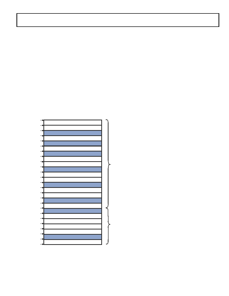
nal memory space is shown in Figure 2.
The on-chip L1 memory system is the highest-performance
memory available to the Blackfin processor. The off-chip mem-
ory system, accessed through the external bus interface unit
(EBIU), provides expansion with SDRAM, flash memory, and
SRAM, optionally accessing up to 132M bytes of
physical memory.
The memory DMA controller provides high bandwidth data-
movement capability. It can perform block transfers of code or
data between the internal memory and the external
memory spaces.
Internal (On-Chip) Memory
The ADSP-BF51x processors have three blocks of on-chip
memory that provide high bandwidth access to the core.
The first block is the L1 instruction memory, consisting of
48K bytes SRAM, of which 16K bytes can be configured as a
four-way set-associative cache. This memory is accessed at full
processor speed.
The second on-chip memory block is the L1 data memory, con-
sisting of up to two banks of up to 32K bytes each. Each memory
bank is configurable, offering both cache and SRAM functional-
ity. This memory block is accessed at full processor speed.
The third memory block is a 4K byte scratchpad SRAM which
runs at the same speed as the L1 memories, but is only accessible
as data SRAM and cannot be configured as cache memory.
External (Off-Chip) Memory
External memory is accessed via the EBIU. This 16-bit interface
provides a glueless connection to a bank of synchronous DRAM
(SDRAM) as well as up to four banks of asynchronous memory
devices including flash, EPROM, ROM, SRAM, and memory
mapped I/O devices.
The SDRAM controller can be programmed to interface to up
to 128M bytes of SDRAM. A separate row can be open for each
SDRAM internal bank, and the SDRAM controller supports up
to four internal SDRAM banks, improving overall performance.
The asynchronous memory controller can be programmed to
control up to four banks of devices with very flexible timing
parameters for a wide variety of devices. Each bank occupies a
1M byte segment regardless of the size of the devices used, so
that these banks are only contiguous if each is fully populated
with 1M byte of memory.
Flash Memory
The ADSP-BF512F/ADSP-BF514F/ADSP-BF516F/
ADSP-BF518F processors contain a SPI flash memory within
the package of the processor and connected to SPI0.
The SPI flash memory has a 4M bit capacity and 1.8V (nominal)
operating voltage. The program/erase endurance is 100,000
cycles per block, and this memory has greater than 100 years of
data retention capability. Also included are support for software
write protection and for fast erase and byte-program.
Figure 2. ADSP-BF51x Internal/External Memory Map
RESERVED
CORE MMR REGISTERS (2M BYTES)
RESERVED
SCRATCHPAD SRAM (4K BYTES)
INSTRUCTION BANK B SRAM (16K BYTES)
SYSTEM MMR REGISTERS (2M BYTES)
RESERVED
DATA BANK B SRAM / CACHE (16K BYTES)
DATA BANK B SRAM (16K BYTES)
DATA BANK A SRAM / CACHE (16K BYTES)
ASYNCMEMORY BANK3 (1M BYTES)
ASYNCMEMORY BANK2 (1M BYTES)
ASYNCMEMORY BANK1 (1M BYTES)
ASYNCMEMORY BANK0 (1M BYTES)
INSTRUCTION BANK C SRAM/CACHE (16K BYTES)
IN
T
ER
N
A
L
M
E
MO
R
Y
M
A
P
E
X
T
E
R
NA
L
M
E
M
O
R
Y
M
A
P
0xFFFF FFFF
0xFFE0 0000
0xFFB0 0000
0xFFA1 4000
0xFFA1 0000
0xFF90 8000
0xFF90 4000
0xFF80 8000
0xFF80 4000
0x2040 0000
0x2030 0000
0x2020 0000
0x2010 0000
0x2000 0000
0xEF00 0000
0x0000 0000
0xFFC0 0000
0xFFB0 1000
0xFFA0 0000
DATA BANK A SRAM (16K BYTES)
0xFF90 0000
0xFF80 0000
RESERVED
0xFFA0 8000
INSTRUCTION BANK A SRAM (16K BYTES)
RESERVED
BOOT ROM (32K BYTES)
0xEF00 8000
RESERVED
0x08 00 0000
0xFFA0 4000
SDRAM MEMORY (16M BYTES - 128M BYTES)
相关PDF资料 |
PDF描述 |
|---|---|
| RBM02DRTN | CONN EDGECARD 4POS DIP .156 SLD |
| MAX6505UTP055+T | IC TEMP SWITCH DL TRIP SOT23-6 |
| RCB120DHNN | CONN EDGECARD 240PS DIP .050 SLD |
| RBM02DRKN | CONN EDGECARD 4POS DIP .156 SLD |
| VI-B5F-EU-B1 | CONVERTER MOD DC/DC 72V 200W |
相关代理商/技术参数 |
参数描述 |
|---|---|
| ADSP-BF518BBCZ4F16 | 功能描述:IC DSP 16/32B 400MHZ 168CSBGA 制造商:analog devices inc. 系列:Blackfin? 包装:带卷(TR) 零件状态:有效 类型:定点 接口:以太网,I2C,PPI,RSI,SPI,SPORT,UART/USART 时钟速率:400MHz 非易失性存储器:FLASH(16Mb) 片载 RAM:116kB 电压 - I/O:1.8V,2.5V,3.3V 电压 - 内核:1.30V 工作温度:-40°C ~ 85°C(TA) 安装类型:表面贴装 封装/外壳:168-LFBGA,CSPBGA 供应商器件封装:168-CSPBGA(12x12) 标准包装:1 |
| ADSP-BF518BBCZ-4F4 | 功能描述:IC DSP 16/32B 400MHZ 168CSPBGA RoHS:是 类别:集成电路 (IC) >> 嵌入式 - DSP(数字式信号处理器) 系列:Blackfin® 标准包装:40 系列:TMS320DM64x, DaVinci™ 类型:定点 接口:I²C,McASP,McBSP 时钟速率:400MHz 非易失内存:外部 芯片上RAM:160kB 电压 - 输入/输出:3.30V 电压 - 核心:1.20V 工作温度:0°C ~ 90°C 安装类型:表面贴装 封装/外壳:548-BBGA,FCBGA 供应商设备封装:548-FCBGA(27x27) 包装:托盘 配用:TMDSDMK642-0E-ND - DEVELPER KIT W/NTSC CAMERA296-23038-ND - DSP STARTER KIT FOR TMS320C6416296-23059-ND - FLASHBURN PORTING KIT296-23058-ND - EVAL MODULE FOR DM642TMDSDMK642-ND - DEVELOPER KIT W/NTSC CAMERA |
| ADSP-BF518BSWZ-4 | 功能描述:IC DSP 16/32B 400MHZ LP 176LQFP RoHS:是 类别:集成电路 (IC) >> 嵌入式 - DSP(数字式信号处理器) 系列:Blackfin® 标准包装:40 系列:TMS320DM64x, DaVinci™ 类型:定点 接口:I²C,McASP,McBSP 时钟速率:400MHz 非易失内存:外部 芯片上RAM:160kB 电压 - 输入/输出:3.30V 电压 - 核心:1.20V 工作温度:0°C ~ 90°C 安装类型:表面贴装 封装/外壳:548-BBGA,FCBGA 供应商设备封装:548-FCBGA(27x27) 包装:托盘 配用:TMDSDMK642-0E-ND - DEVELPER KIT W/NTSC CAMERA296-23038-ND - DSP STARTER KIT FOR TMS320C6416296-23059-ND - FLASHBURN PORTING KIT296-23058-ND - EVAL MODULE FOR DM642TMDSDMK642-ND - DEVELOPER KIT W/NTSC CAMERA |
| ADSP-BF518BSWZ4F16 | 功能描述:IC DSP 16/32B 400MHZ LP 176LQFP 制造商:analog devices inc. 系列:Blackfin? 包装:托盘 零件状态:有效 类型:定点 接口:以太网,I2C,PPI,RSI,SPI,SPORT,UART/USART 时钟速率:400MHz 非易失性存储器:FLASH(16Mb) 片载 RAM:116kB 电压 - I/O:1.8V,2.5V,3.3V 电压 - 内核:1.30V 工作温度:-40°C ~ 85°C(TA) 安装类型:表面贴装 封装/外壳:176-LQFP 裸露焊盘 供应商器件封装:176-LQFP-EP(24x24) 标准包装:1 |
| ADSP-BF518BSWZ-4F4 | 功能描述:IC DSP 16/32B 400MHZ LP 176LQFP RoHS:是 类别:集成电路 (IC) >> 嵌入式 - DSP(数字式信号处理器) 系列:Blackfin® 标准包装:2 系列:StarCore 类型:SC140 内核 接口:DSI,以太网,RS-232 时钟速率:400MHz 非易失内存:外部 芯片上RAM:1.436MB 电压 - 输入/输出:3.30V 电压 - 核心:1.20V 工作温度:-40°C ~ 105°C 安装类型:表面贴装 封装/外壳:431-BFBGA,FCBGA 供应商设备封装:431-FCPBGA(20x20) 包装:托盘 |
发布紧急采购,3分钟左右您将得到回复。