- 您现在的位置:买卖IC网 > PDF目录19388 > ADSP-BF525KBCZ-6 (Analog Devices Inc)IC DSP CTRLR 16B 600MHZ 289BGA PDF资料下载
参数资料
| 型号: | ADSP-BF525KBCZ-6 |
| 厂商: | Analog Devices Inc |
| 文件页数: | 17/88页 |
| 文件大小: | 0K |
| 描述: | IC DSP CTRLR 16B 600MHZ 289BGA |
| 产品变化通告: | Datasheet Specification Change 14/Dec/2009 |
| 标准包装: | 1 |
| 系列: | Blackfin® |
| 类型: | 定点 |
| 接口: | DMA,I²C,PPI,SPI,SPORT,UART,USB |
| 时钟速率: | 600MHz |
| 非易失内存: | ROM(32 kB) |
| 芯片上RAM: | 132kB |
| 电压 - 输入/输出: | 1.8V,2.5V,3.3V |
| 电压 - 核心: | 1.10V |
| 工作温度: | 0°C ~ 70°C |
| 安装类型: | 表面贴装 |
| 封装/外壳: | 289-LFBGA,CSPBGA |
| 供应商设备封装: | 289-CSPBGA(12x12) |
| 包装: | 托盘 |
第1页第2页第3页第4页第5页第6页第7页第8页第9页第10页第11页第12页第13页第14页第15页第16页当前第17页第18页第19页第20页第21页第22页第23页第24页第25页第26页第27页第28页第29页第30页第31页第32页第33页第34页第35页第36页第37页第38页第39页第40页第41页第42页第43页第44页第45页第46页第47页第48页第49页第50页第51页第52页第53页第54页第55页第56页第57页第58页第59页第60页第61页第62页第63页第64页第65页第66页第67页第68页第69页第70页第71页第72页第73页第74页第75页第76页第77页第78页第79页第80页第81页第82页第83页第84页第85页第86页第87页第88页
�� �
�
�ADSP-BF522/ADSP-BF523/ADSP-BF524/ADSP-BF525/ADSP-BF526/ADSP-BF527�
�specified� by� the� crystal� manufacturer.� The� user� should� verify� the�
�customized� values� based� on� careful� investigations� on� multiple�
�devices� over� temperature� range.�
�BLACKFIN�
�CLKOUT�
�TO� PLL� CIRCUITRY�
�permitted� to� run� up� to� the� frequency� specified� by� the� part’s�
�maximum� instruction� rate.� The� CLKOUT� pin� reflects� the� SCLK�
�frequency� to� the� off-chip� world.� It� is� part� of� the� SDRAM� inter-�
�face,� but� it� functions� as� a� reference� signal� in� other� timing�
�specifications� as� well.� While� active� by� default,� it� can� be� disabled�
�using� the� EBIU_SDGCTL� and� EBIU_AMGCTL� registers.�
�“FINE”� ADJUSTMENT�
�“COARSE”� ADJUSTMENT�
�CLKBUF�
�EN�
�REQUIRES� PLL� SEQUENCING�
�ON-THE-FLY�
�560�
�÷� 1,� 2,� 4,� 8�
�CCLK�
�EN�
�CLKIN�
�330�
�*�
�XTAL�
�FOR� OVERTONE�
�CLKIN�
�PLL�
�5� to� 64�
�VCO�
�÷� 1� to� 15�
�SCLK�
�OPERATION� ONLY:�
�18� pF� *�
�18� pF� *�
�SCLK�
�CCLK�
�Figure� 7.� Frequency� Modification� Methods�
�NOTE:� VALUES� MARKED� WITH� *� MUST� BE� CUSTOMIZED,� DEPENDING�
�ON� THE� CRYSTAL� AND� LAYOUT.� PLEASE� ANALYZE� CAREFULLY.� FOR�
�FREQUENCIES� ABOVE� 33� MHz,� THE� SUGGESTED� CAPACITOR� VALUE�
�OF� 18� pF� SHOULD� BE� TREATED� AS� A� MAXIMUM,� AND� THE� SUGGESTED�
�RESISTOR� VALUE� SHOULD� BE� REDUCED� TO� 0� .�
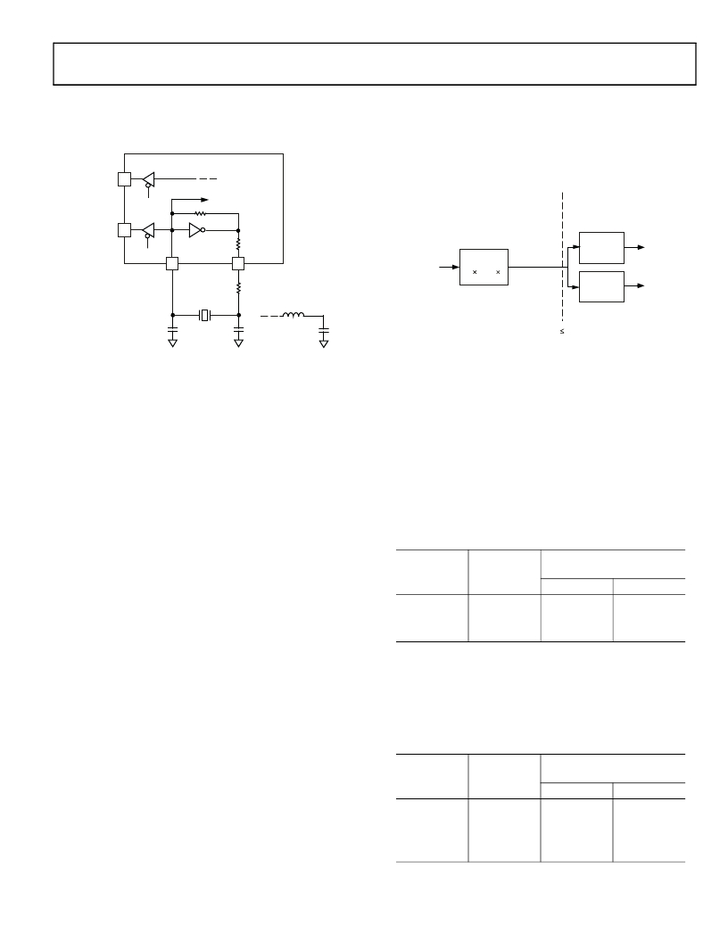
�Figure� 6.� External� Crystal� Connections�
�A� third-overtone� crystal� can� be� used� for� frequencies� above�
�25� MHz.� The� circuit� is� then� modified� to� ensure� crystal� operation�
�only� at� the� third� overtone� by� adding� a� tuned� inductor� circuit� as�
�shown� in� Figure� 6� .� A� design� procedure� for� third-overtone� oper-�
�ation� is� discussed� in� detail� in� application� note� (EE-168)� Using�
�Third� Overtone� Crystals� with� the� ADSP-218x� DSP� on� the� Analog�
�Devices� website� (� www.analog.com� )—use� site� search� on�
�“EE-168.”�
�All� on-chip� peripherals� are� clocked� by� the� system� clock� (SCLK).�
�The� system� clock� frequency� is� programmable� by� means� of� the�
�SSEL3–0� bits� of� the� PLL_DIV� register.� The� values� programmed�
�into� the� SSEL� fields� define� a� divide� ratio� between� the� PLL� output�
�(VCO)� and� the� system� clock.� SCLK� divider� values� are� 1� through�
�15.� Table� 6� illustrates� typical� system� clock� ratios.�
�Note� that� the� divisor� ratio� must� be� chosen� to� limit� the� system�
�clock� frequency� to� its� maximum� of� f� SCLK� .� The� SSEL� value� can� be�
�dynamically� changed� without� any� PLL� lock� latencies� by� writing�
�the� appropriate� values� to� the� PLL� divisor� register� (PLL_DIV)�
�using� the� bfrom_SysControl()� function� in� the� on-chip� ROM.�
�Table� 6.� Example� System� Clock� Ratios�
�The� CLKBUF� pin� is� an� output� pin,� which� is� a� buffered� version�
�of� the� input� clock.� This� pin� is� particularly� useful� in� Ethernet�
�applications� to� limit� the� number� of� required� clock� sources� in� the�
�system.� In� this� type� of� application,� a� single� 25� MHz� or� 50� MHz�
�crystal� may� be� applied� directly� to� the� processor.� The� 25� MHz� or�
�50� MHz� output� of� CLKBUF� can� then� be� connected� to� an� exter-�
�nal� Ethernet� MII� or� RMII� PHY� device.� If,� instead� of� a� crystal,� an�
�external� oscillator� is� used� at� CLKIN,� CLKBUF� will� not� have� the�
�Signal� Name�
�SSEL3–0�
�0001�
�0110�
�1010�
�Divider� Ratio�
�VCO/SCLK�
�1:1�
�6:1�
�10:1�
�Example� Frequency� Ratios�
�(MHz)�
�VCO� SCLK�
�100� 100�
�300� 50�
�500� 50�
�40/60� duty� cycle� required� by� some� devices.� The� CLKBUF� output�
�is� active� by� default� and� can� be� disabled� for� power� savings� rea-�
�sons� using� the� VR_CTL� register.�
�The� Blackfin� core� runs� at� a� different� clock� rate� than� the� on-chip�
�peripherals.� As� shown� in� Figure� 7� ,� the� core� clock� (CCLK)� and�
�system� peripheral� clock� (SCLK)� are� derived� from� the� input�
�clock� (CLKIN)� signal.� An� on-chip� PLL� is� capable� of� multiplying�
�the� CLKIN� signal� by� a� programmable� multiplication� factor�
�(bounded� by� specified� minimum� and� maximum� VCO� frequen-�
�The� core� clock� (CCLK)� frequency� can� also� be� dynamically�
�changed� by� means� of� the� CSEL1–0� bits� of� the� PLL_DIV� register.�
�Supported� CCLK� divider� ratios� are� 1,� 2,� 4,� and� 8,� as� shown� in�
��fast� core� frequency� modifications.�
�Table� 7.� Core� Clock� Ratios�
�Example� Frequency� Ratios�
�cies).� The� default� multiplier� can� be� modified� by� a� software�
�instruction� sequence.� This� sequence� is� managed� by� the�
�bfrom_SysControl()� function� in� the� on-chip� ROM.�
�On-the-fly� CCLK� and� SCLK� frequency� changes� can� be� applied�
�by� using� the� bfrom_SysControl()� function� in� the� on-chip� ROM.�
�The� maximum� allowed� CCLK� and� SCLK� rates� depend� on� the�
�applied� voltages� V� DDINT� ,� V� DDEXT� ,� and� V� DDMEM� ;� the� VCO� is� always�
�Signal� Name�
�CSEL1–0�
�00�
�01�
�10�
�11�
�Divider� Ratio�
�VCO/CCLK�
�1:1�
�2:1�
�4:1�
�8:1�
�(MHz)�
�VCO� CCLK�
�300� 300�
�300� 150�
�500� 125�
�200� 25�
�Rev.� D� |�
�Page� 17� of� 88� |� July� 2013�
�相关PDF资料 |
PDF描述 |
|---|---|
| ADSP-BF533SBBC-5V | IC DSP CTLR DUAL 160CSPBGA |
| SWS60015 | PWR SUP 15V 40A SNG OUTPUT |
| ADSP-BF537BBCZ-5B | IC DSP CTLR 16BIT 208CSPBGA |
| ADSP-BF534YBCZ-4B | IC DSP CTLR 16BIT 400MHZ 208-CSP |
| ADSP-21488BSWZ-3A | IC DSP 3MBIT 400MHZ 100LQFP |
相关代理商/技术参数 |
参数描述 |
|---|---|
| ADSP-BF525KBCZ-6A | 功能描述:IC DSP 16BIT 600MHZ 208CSPBGA RoHS:是 类别:集成电路 (IC) >> 嵌入式 - DSP(数字式信号处理器) 系列:Blackfin® 标准包装:40 系列:TMS320DM64x, DaVinci™ 类型:定点 接口:I²C,McASP,McBSP 时钟速率:400MHz 非易失内存:外部 芯片上RAM:160kB 电压 - 输入/输出:3.30V 电压 - 核心:1.20V 工作温度:0°C ~ 90°C 安装类型:表面贴装 封装/外壳:548-BBGA,FCBGA 供应商设备封装:548-FCBGA(27x27) 包装:托盘 配用:TMDSDMK642-0E-ND - DEVELPER KIT W/NTSC CAMERA296-23038-ND - DSP STARTER KIT FOR TMS320C6416296-23059-ND - FLASHBURN PORTING KIT296-23058-ND - EVAL MODULE FOR DM642TMDSDMK642-ND - DEVELOPER KIT W/NTSC CAMERA |
| ADSP-BF525KBCZ-6C2 | 功能描述:IC DSP 16BIT 600MHZ 289CSPBGA RoHS:是 类别:集成电路 (IC) >> 嵌入式 - DSP(数字式信号处理器) 系列:Blackfin® 标准包装:40 系列:TMS320DM64x, DaVinci™ 类型:定点 接口:I²C,McASP,McBSP 时钟速率:400MHz 非易失内存:外部 芯片上RAM:160kB 电压 - 输入/输出:3.30V 电压 - 核心:1.20V 工作温度:0°C ~ 90°C 安装类型:表面贴装 封装/外壳:548-BBGA,FCBGA 供应商设备封装:548-FCBGA(27x27) 包装:托盘 配用:TMDSDMK642-0E-ND - DEVELPER KIT W/NTSC CAMERA296-23038-ND - DSP STARTER KIT FOR TMS320C6416296-23059-ND - FLASHBURN PORTING KIT296-23058-ND - EVAL MODULE FOR DM642TMDSDMK642-ND - DEVELOPER KIT W/NTSC CAMERA |
| ADSP-BF526BBCZ3 | 制造商:Analog Devices 功能描述: |
| ADSP-BF526BBCZ-3A | 功能描述:EMBEDDED PROCESSOR, BLACKFIN RoHS:是 类别:集成电路 (IC) >> 嵌入式 - DSP(数字式信号处理器) 系列:Blackfin® 标准包装:2 系列:StarCore 类型:SC140 内核 接口:DSI,以太网,RS-232 时钟速率:400MHz 非易失内存:外部 芯片上RAM:1.436MB 电压 - 输入/输出:3.30V 电压 - 核心:1.20V 工作温度:-40°C ~ 105°C 安装类型:表面贴装 封装/外壳:431-BFBGA,FCBGA 供应商设备封装:431-FCPBGA(20x20) 包装:托盘 |
| ADSP-BF526BBCZ-3AX | 制造商:Analog Devices 功能描述:DSP 32BIT 300MHZ 208CSPBGA - Trays |
发布紧急采购,3分钟左右您将得到回复。