- 您现在的位置:买卖IC网 > PDF目录19394 > ADSP21262SKBCZ200R (Analog Devices Inc)IC DSP CTLR 32BIT 136CSPBGA PDF资料下载
参数资料
| 型号: | ADSP21262SKBCZ200R |
| 厂商: | Analog Devices Inc |
| 文件页数: | 17/60页 |
| 文件大小: | 0K |
| 描述: | IC DSP CTLR 32BIT 136CSPBGA |
| 产品培训模块: | SHARC Processor Overview |
| 标准包装: | 1 |
| 系列: | SHARC® |
| 类型: | 定点/浮点 |
| 接口: | DAI,SPI |
| 时钟速率: | 200MHz |
| 非易失内存: | ROM(512 kB) |
| 芯片上RAM: | 256kB |
| 电压 - 输入/输出: | 3.30V |
| 电压 - 核心: | 1.20V |
| 工作温度: | 0°C ~ 70°C |
| 安装类型: | 表面贴装 |
| 封装/外壳: | 136-LFBGA,CSPBGA |
| 供应商设备封装: | 136-CSPBGA(12x12) |
| 包装: | 标准包装 |
| 其它名称: | ADSP21262SKBCZ200RDKR |
第1页第2页第3页第4页第5页第6页第7页第8页第9页第10页第11页第12页第13页第14页第15页第16页当前第17页第18页第19页第20页第21页第22页第23页第24页第25页第26页第27页第28页第29页第30页第31页第32页第33页第34页第35页第36页第37页第38页第39页第40页第41页第42页第43页第44页第45页第46页第47页第48页第49页第50页第51页第52页第53页第54页第55页第56页第57页第58页第59页第60页
�� �
�
�ADSP-21362/ADSP-21363/ADSP-21364/ADSP-21365/ADSP-21366�
�?� The� product� of� CLKIN� and� PLLM� must� never� exceed� 1/2�
�f� VCO� (max)� in� Table� 11� if� the� input� divider� is� not� enabled�
�(INDIV� =� 0).�
�?� The� product� of� CLKIN� and� PLLM� must� never� exceed� f� VCO�
�(max)� in� Table� 11� if� the� input� divider� is� enabled�
�(INDIV� =� 1).�
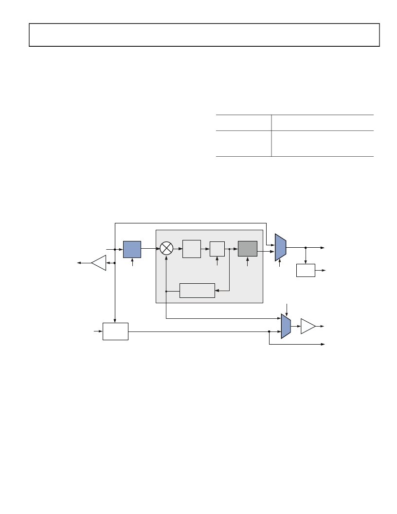
�The� VCO� frequency� is� calculated� as� follows:�
�f� VCO� =� 2� � PLLM� � f� INPUT�
�f� CCLK� =� (2� ×� PLLM� ×� f� INPUT� )� ÷� (2� ×� PLLN� )�
�f� INPUT� =� CLKIN� ÷� 2� when� the� input� divider� is� enabled�
�Note� the� definitions� of� the� clock� periods� that� are� a� function� of�
�CLKIN� and� the� appropriate� ratio� control� shown� in� Table� 9� .� All�
�of� the� timing� specifications� for� the� ADSP-2136x� peripherals� are�
�defined� in� relation� to� t� PCLK� .� Refer� to� the� peripheral� specific� sec-�
�tion� for� each� peripheral’s� timing� information.�
�Table� 9.� Clock� Periods�
�Timing�
�where:�
�f� VCO� =� VCO� output�
�PLLM� =� Multiplier� value� programmed� in� the� PMCTL� register.�
�During� reset,� the� PLLM� value� is� derived� from� the� ratio� selected�
�Requirements�
�t� CK�
�t� CCLK�
�t� PCLK�
�Description�
�CLKIN� Clock� Period�
�Processor� Core� Clock� Period�
�Peripheral� Clock� Period� =� 2� � t� CCLK�
�using� the� CLK_CFG� pins� in� hardware.�
�PLLN� =� 1,� 2,� 4,� 8� based� on� the� PLLD� value� programmed� on� the�
�PMCTL� register.� During� reset� this� value� is� 1.�
�f� INPUT� =� Input� frequency� to� the� PLL.�
�f� INPUT� =� CLKIN� when� the� input� divider� is� disabled� or�
�PLL�
��lator� or� crystal.� The� shaded� divider/multiplier� blocks� denote�
�where� clock� ratios� can� be� set� through� hardware� or� software�
�using� the� power� management� control� register� (PMCTL).� For�
�more� information,� refer� to� the� ADSP-2136x� SHARC� Processor�
�Hardware� Reference� .�
�CLKIN�
�CLKIN�
�DIVIDER�
�f� INPUT�
�LOOP�
�FILTER�
�VCO�
�f� VCO�
�PLL�
�DIVIDER�
�f� CCLK�
�CCLK�
�XTAL�
�BUF�
�PMCTL�
�(INDIV)�
�CLK_CFGx/�
�PMCTL� (2� � PLLM)�
�PMCTL�
�(2� � PLLN)�
�PMCTL�
�(PLLBP)�
�DIVIDE�
�BY� 2�
�PCLK�
�f� VCO� ÷� (2� ×� PLLM)�
�PMCTL� (CLKOUTEN)�
�CLKOUT� (TEST� ONLY)*�
�RESETOUT�
�RESET�
�DELAY� OF�
�4096� CLKIN�
�RESETOUT�
�BUF�
�CYCLES�
�CORERST�
�*CLKOUT� (TEST� ONLY)� FREQUENCY� IS� THE� SAME� AS� f� INPUT.�
�THIS� SIGNAL� IS� NOT� SPECIFIED� OR� SUPPORTED� FOR� ANY� DESIGN.�
�Figure� 5.� Core� Clock� and� System� Clock� Relationship� to� CLKIN�
�Rev.� J� |�
�Page� 17� of� 60� |�
�July� 2013�
�相关PDF资料 |
PDF描述 |
|---|---|
| MAX6505UTP080+T | IC TEMP SWITCH DL TRIP SOT23-6 |
| RW2-2405D/H3/B | CONV DC/DC 2W 18-36VIN +/-05VOUT |
| F910J337KNC | CAP TANT 330UF 6.3V 10% 2917 |
| TAP106J035SCS | CAP TANT 10UF 35V 5% RADIAL |
| VI-B5H-EU-B1 | CONVERTER MOD DC/DC 52V 200W |
相关代理商/技术参数 |
参数描述 |
|---|---|
| ADSP-21262SKSTZ200 | 功能描述:IC DSP CONTROLLER 32BIT 144-LQFP RoHS:是 类别:集成电路 (IC) >> 嵌入式 - DSP(数字式信号处理器) 系列:SHARC® 标准包装:40 系列:TMS320DM64x, DaVinci™ 类型:定点 接口:I²C,McASP,McBSP 时钟速率:400MHz 非易失内存:外部 芯片上RAM:160kB 电压 - 输入/输出:3.30V 电压 - 核心:1.20V 工作温度:0°C ~ 90°C 安装类型:表面贴装 封装/外壳:548-BBGA,FCBGA 供应商设备封装:548-FCBGA(27x27) 包装:托盘 配用:TMDSDMK642-0E-ND - DEVELPER KIT W/NTSC CAMERA296-23038-ND - DSP STARTER KIT FOR TMS320C6416296-23059-ND - FLASHBURN PORTING KIT296-23058-ND - EVAL MODULE FOR DM642TMDSDMK642-ND - DEVELOPER KIT W/NTSC CAMERA |
| ADSP-21262SKSTZ200 | 制造商:Analog Devices 功能描述:IC 32-BIT DSP |
| ADSP-21266 | 制造商:AD 制造商全称:Analog Devices 功能描述:SHARC Embedded Processor |
| ADSP-21266_07 | 制造商:AD 制造商全称:Analog Devices 功能描述:Embedded Processor |
| ADSP-21266KSTZ-1C | 制造商:Analog Devices 功能描述:- Trays |
发布紧急采购,3分钟左右您将得到回复。