参数资料
| 型号: | ADUC814BRU |
| 厂商: | Analog Devices Inc |
| 文件页数: | 18/72页 |
| 文件大小: | 0K |
| 描述: | IC ADC 12BIT W/FLASH MCU 28TSSOP |
| 标准包装: | 50 |
| 系列: | MicroConverter® ADuC8xx |
| 核心处理器: | 8052 |
| 芯体尺寸: | 8-位 |
| 速度: | 16.78MHz |
| 连通性: | I²C,SPI,UART/USART |
| 外围设备: | POR,PSM,温度传感器,WDT |
| 输入/输出数: | 17 |
| 程序存储器容量: | 8KB(8K x 8) |
| 程序存储器类型: | 闪存 |
| EEPROM 大小: | 640 x 8 |
| RAM 容量: | 256 x 8 |
| 电压 - 电源 (Vcc/Vdd): | 2.7 V ~ 5.5 V |
| 数据转换器: | A/D 6x12b; D/A 2x12b |
| 振荡器型: | 内部 |
| 工作温度: | -40°C ~ 125°C |
| 封装/外壳: | 28-TSSOP(0.173",4.40mm 宽) |
| 包装: | 管件 |
| 配用: | EVAL-ADUC814QSZ-ND - KIT DEV FOR ADUC814 MICROCONVRTR |
第1页第2页第3页第4页第5页第6页第7页第8页第9页第10页第11页第12页第13页第14页第15页第16页第17页当前第18页第19页第20页第21页第22页第23页第24页第25页第26页第27页第28页第29页第30页第31页第32页第33页第34页第35页第36页第37页第38页第39页第40页第41页第42页第43页第44页第45页第46页第47页第48页第49页第50页第51页第52页第53页第54页第55页第56页第57页第58页第59页第60页第61页第62页第63页第64页第65页第66页第67页第68页第69页第70页第71页第72页
ADuC814
Rev. A | Page 25 of 72
DRIVING THE ADC
The ADC incorporates a successive approximation architecture
(SAR) involving a charge-sampled input stage. Each ADC con-
version is divided into two distinct phases as defined by the
position of the switches in Figure 25. During the sampling
phase (with SW1 and SW2 in the track position), a charge
proportional to the voltage on the analog input is developed
across the input sampling capacitor. During the conversion
phase (with both switches in the hold position), the capacitor
DAC is adjusted via internal SAR logic until the voltage on
Node A is zero, indicating that the sampled charge on the input
capacitor is balanced out by the charge being output by the
capacitor DAC. The digital value finally contained in the SAR is
then latched out as the result of the ADC conversion. Control of
the SAR, and timing of acquisition and sampling modes, is han-
dled automatically by built-in ADC control logic. Acquisition and
conversion times are also fully configurable under user control.
COMPARATOR
VREF
AGND
DAC1
DAC0
TEMPERATURE MONITOR
INTERNAL
CHANNELS
AIN5
AIN0
32pF
AGND
ADuC814
TRACK
HOLD
200
200
02748-A
-032
CAPACITOR
DAC
Figure 25. Internal ADC Structure
Note that whenever a new input channel is selected, a residual
charge from the 32 pF sampling capacitor places a transient on
the newly selected input. The signal source must be capable of
recovering from this transient before the sampling switches
click into hold mode. Delays can be inserted in software
(between channel selection and conversion request) to account
for input stage settling, but a hardware solution alleviates this
burden from the software design task and ultimately results in a
cleaner system implementation.
One hardware solution is to choose a very fast settling op amp
to drive each analog input. Such an op amp would need to fully
settle from a small signal transient in less than 300 ns in order
to guarantee adequate settling under all software configurations.
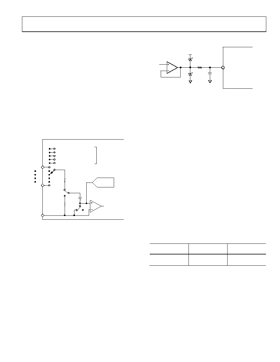
A better solution, recommended for use with any amplifier, is
shown in Figure 26.
AIN0
ADuC814
10
0.1
F
02748-A
-033
Figure 26. Buffering Analog Inputs
At first glance the circuit in Figure 26 may look like a simple
anti-aliasing filter, it actually serves no such purpose. Though
the R/C does help to reject some incoming high frequency noise,
its primary function is to ensure that the transient demands of
the ADC input stage are met. It does so by providing a capacitive
bank from which the 32 pF sampling capacitor can draw its
charge. Since the 0.1 F capacitor in Figure 26 is more than
3000 times the size of the 32 pF sampling capacitor, its voltage
does not change by more than one count of the 12-bit transfer
function when the 32 pF charge from a previous channel is
dumped onto it. A larger capacitor can be used if desired, but
care needs to be taken if choosing a larger resistor (see Table 9).
The Schottky diodes in Figure 26 may be necessary to limit the
voltage applied to the analog input pin as per the Absolute
Maximum Ratings. They are not necessary if the op amp is
powered from the same supply as the ADuC814 because, in that
case, the op amp is unable to generate voltages above VDD or
below ground. An op amp of some kind is necessary unless the
signal source is very low impedance to begin with. DC leakage
currents at the ADuC814 analog inputs can cause measurable
dc errors with external source impedances as little as 100 or
so. To ensure accurate ADC operation, keep the total source
impedance at each analog input less than 61 . Table 9 illustrates
examples of how source impedance can affect dc accuracy.
Table 9. Source Impedance Errors
Source
Impedance
Error from 1 A
Leakage Current
Error from 10 A
Leakage Current
61
61 V = 0.1 LSB
610 V = 1 LSB
610
610 V = 1 LSB
6.1 mV = 10 LSB
Although Figure 26 shows the op amp operating at a gain of 1,
you can configure it for any gain needed. Also, you can just as
easily use an instrumentation amplifier in its place to condition
differential signals. Use any modern amplifier that is capable of
delivering the signal (0 V to VREF) with minimal saturation.
Some single-supply, rail-to-rail op-amps that are useful for this
purpose include, but are certainly not limited to, the ones given
in Table 10. Check the Analog Devices literature (CD ROM data
book, etc.) for details on these and other op amps and
instrumentation amps.
相关PDF资料 |
PDF描述 |
|---|---|
| ADUC816BCP | IC MCU 8K FLASH ADC/DAC 56LFCSP |
| ADUC824BSZ-REEL | IC MCU 8K FLASH ADC/DAC 52MQFP |
| ADUC831BCPZ | IC MCU 62K FLASH ADC/DAC 56LFCSP |
| ADUC832BSZ-REEL | IC MCU 62K FLASH ADC/DAC 52MQFP |
| ADUC834BCPZ-REEL | IC MCU 62K FLASH ADC/DAC 56LFCSP |
相关代理商/技术参数 |
参数描述 |
|---|---|
| ADUC814BRU-REEL | 制造商:Analog Devices 功能描述:MCU 8-bit ADuC8xx 8052 CISC 8KB Flash 3V/5V 28-Pin TSSOP T/R 制造商:Analog Devices 功能描述:MCU 8BIT CISC 8KB FLASH 3.3V/5V 28TSSOP - Tape and Reel 制造商:Analog Devices Inc. 功能描述:8-bit Microcontrollers - MCU 12 BIT ADC WITH EMBEDDED 8-BIT MICRO I.C |
| ADUC814BRU-REEL7 | 制造商:Analog Devices 功能描述:MCU 8-Bit ADuC8xx 8052 CISC 8KB Flash 3V/5V 28-Pin TSSOP T/R 制造商:Analog Devices 功能描述:MCU 8BIT CISC 8KB FLASH 3.3V/5V 28TSSOP - Tape and Reel 制造商:Analog Devices Inc. 功能描述:8-bit Microcontrollers - MCU 12 BIT ADC WITH EMBEDDED 8-BIT MICRO I.C |
| ADUC814BRUZ | 功能描述:IC ADC 12BIT W/FLASH MCU 28TSSOP RoHS:是 类别:集成电路 (IC) >> 嵌入式 - 微控制器, 系列:MicroConverter® ADuC8xx 产品培训模块:MCU Product Line Introduction XMEGA Introduction AVR XMEGA USB Connectivity 标准包装:90 系列:AVR® XMEGA 核心处理器:AVR 芯体尺寸:8/16-位 速度:32MHz 连通性:I²C,IrDA,SPI,UART/USART 外围设备:欠压检测/复位,DMA,POR,PWM,WDT 输入/输出数:50 程序存储器容量:192KB(96K x 16) 程序存储器类型:闪存 EEPROM 大小:4K x 8 RAM 容量:16K x 8 电压 - 电源 (Vcc/Vdd):1.6 V ~ 3.6 V 数据转换器:A/D 16x12b; D/A 2x12b 振荡器型:内部 工作温度:-40°C ~ 85°C 封装/外壳:64-TQFP 包装:托盘 配用:ATSTK600-RC14-ND - STK600 SOCKET/ADAPTER 64TQFPATSTK600-TQFP64-ND - STK600 SOCKET/ADAPTER 64-TQFPATAVRONEKIT-ND - KIT AVR/AVR32 DEBUGGER/PROGRMMRATAVRISP2-ND - PROGRAMMER AVR IN SYSTEM |
| ADUC814BRUZ-REEL | 功能描述:IC MCU 8K FLASH ADC/DAC 28-TSSOP RoHS:是 类别:集成电路 (IC) >> 嵌入式 - 微控制器, 系列:MicroConverter® ADuC8xx 标准包装:38 系列:Encore!® XP® 核心处理器:eZ8 芯体尺寸:8-位 速度:5MHz 连通性:IrDA,UART/USART 外围设备:欠压检测/复位,LED,POR,PWM,WDT 输入/输出数:16 程序存储器容量:4KB(4K x 8) 程序存储器类型:闪存 EEPROM 大小:- RAM 容量:1K x 8 电压 - 电源 (Vcc/Vdd):2.7 V ~ 3.6 V 数据转换器:- 振荡器型:内部 工作温度:-40°C ~ 105°C 封装/外壳:20-SOIC(0.295",7.50mm 宽) 包装:管件 其它名称:269-4116Z8F0413SH005EG-ND |
| ADUC814BRUZ-REEL7 | 功能描述:IC MCU 8K FLASH ADC/DAC 28-TSSOP RoHS:是 类别:集成电路 (IC) >> 嵌入式 - 微控制器, 系列:MicroConverter® ADuC8xx 标准包装:38 系列:Encore!® XP® 核心处理器:eZ8 芯体尺寸:8-位 速度:5MHz 连通性:IrDA,UART/USART 外围设备:欠压检测/复位,LED,POR,PWM,WDT 输入/输出数:16 程序存储器容量:4KB(4K x 8) 程序存储器类型:闪存 EEPROM 大小:- RAM 容量:1K x 8 电压 - 电源 (Vcc/Vdd):2.7 V ~ 3.6 V 数据转换器:- 振荡器型:内部 工作温度:-40°C ~ 105°C 封装/外壳:20-SOIC(0.295",7.50mm 宽) 包装:管件 其它名称:269-4116Z8F0413SH005EG-ND |
发布紧急采购,3分钟左右您将得到回复。