参数资料
| 型号: | ADUC831BCPZ |
| 厂商: | Analog Devices Inc |
| 文件页数: | 60/76页 |
| 文件大小: | 0K |
| 描述: | IC MCU 62K FLASH ADC/DAC 56LFCSP |
| 标准包装: | 1 |
| 系列: | MicroConverter® ADuC8xx |
| 核心处理器: | 8052 |
| 芯体尺寸: | 8-位 |
| 速度: | 16MHz |
| 连通性: | EBI/EMI,I²C,SPI,UART/USART |
| 外围设备: | PSM,温度传感器,WDT |
| 输入/输出数: | 34 |
| 程序存储器容量: | 62KB(62K x 8) |
| 程序存储器类型: | 闪存 |
| EEPROM 大小: | 4K x 8 |
| RAM 容量: | 2.25K x 8 |
| 电压 - 电源 (Vcc/Vdd): | 2.7 V ~ 5.5 V |
| 数据转换器: | A/D 8x12b,D/A 2x12b |
| 振荡器型: | 内部 |
| 工作温度: | -40°C ~ 85°C |
| 封装/外壳: | 56-VFQFN 裸露焊盘,CSP |
| 包装: | 托盘 |
| 配用: | EVAL-ADUC831QSZ-ND - KIT DEV FOR ADUC831 QUICK START |
第1页第2页第3页第4页第5页第6页第7页第8页第9页第10页第11页第12页第13页第14页第15页第16页第17页第18页第19页第20页第21页第22页第23页第24页第25页第26页第27页第28页第29页第30页第31页第32页第33页第34页第35页第36页第37页第38页第39页第40页第41页第42页第43页第44页第45页第46页第47页第48页第49页第50页第51页第52页第53页第54页第55页第56页第57页第58页第59页当前第60页第61页第62页第63页第64页第65页第66页第67页第68页第69页第70页第71页第72页第73页第74页第75页第76页
REV. 0
ADuC831
–63–
128ms TYP
1.0V TYP
128ms TYP
2.45V TYP
1.0V TYP
INTERNAL
CORE RESET
DVDD
Figure 62. Internal POR Operation
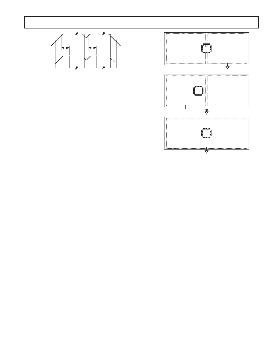
Grounding and Board Layout Recommendations
As with all high resolution data converters, special attention must
be paid to grounding and PC board layout of ADuC831-based
designs in order to achieve optimum performance from the
ADC and DACs.
Although the ADuC831 has separate pins for analog and digital
ground (AGND and DGND), the user must not tie these to two
separate ground planes unless the two ground planes are con-
nected together very close to the ADuC831, as illustrated in the
simplified example of Figure 63a. In systems where digital and
analog ground planes are connected together somewhere else
(at the system’s power supply for example), they cannot be con-
nected again near the ADuC831 since a ground loop would result.
In these cases, tie the ADuC831’s AGND and DGND pins all
to the analog ground plane, as illustrated in Figure 63b. In systems
with only one ground plane, ensure that the digital and analog
components are physically separated onto separate halves of the
board such that digital return currents do not flow near analog
circuitry and vice versa. The ADuC831 can then be placed between
the digital and analog sections, as illustrated in Figure 63c.
In all of these scenarios, and in more complicated real-life applica-
tions, keep in mind the flow of current from the supplies and back
to ground. Make sure the return paths for all currents are as
close as possible to the paths the currents took to reach their desti-
nations. For example, do not power components on the analog
side of Figure 63b with DVDD since that would force return currents
from DVDD to flow through AGND. Also, try to avoid digital
currents flowing under analog circuitry, which could happen if
the user placed a noisy digital chip on the left half of the board in
Figure 63c. Whenever possible, avoid large discontinuities in the
ground plane(s) (such as are formed by a long trace on the same
layer), since they force return signals to travel a longer path. And
of course, make all connections to the ground plane directly,
with little or no trace separating the pin from its via to ground.
Note that the bottom paddle of the CSP package should not
be connected to ground. It should be left unconnected.
If the user plans to connect fast logic signals (rise/fall time < 5 ns) to
any of the ADuC831’s digital inputs, add a series resistor to each
relevant line to keep rise and fall times longer than 5 ns at the
ADuC831 input pins. A value of 100
or 200 is usually suffi-
cient to prevent high speed signals from coupling capacitively into
the ADuC831 and affecting the accuracy of ADC conversions.
DGND
AGND
PLACE ANALOG
COMPONENTS
HERE
PLACE DIGITAL
COMPONENTS
HERE
GND
PLACE ANALOG
COMPONENTS
HERE
PLACE DIGITAL
COMPONENTS
HERE
DGND
a.
AGND
PLACE ANALOG
COMPONENTS
HERE
PLACE DIGITAL
COMPONENTS
HERE
b.
c.
Figure 63. System Grounding Schemes
OTHER HARDWARE CONSIDERATIONS
To facilitate in-circuit programming, plus in-circuit debug and
emulation options, users will want to implement some simple
connection points in their hardware that will allow easy access
to download, debug, and emulation modes.
In-Circuit Serial Download Access
Nearly all ADuC831 designs will want to take advantage of the
in-circuit reprogrammability of the chip. This is accomplished by
a connection to the ADuC831’s UART, which requires an exter-
nal RS-232 chip for level translation if downloading code from
a PC. Basic configuration of an RS-232 connection is illustrated
in Figure 66 with a simple ADM202-based circuit. If users would
rather not design an RS-232 chip onto a board, refer to the
application note “uC006–A 4-Wire UART-to-PC Interface”
* for
a simple (and zero-cost-per-board) method of gaining in-circuit
serial download access to the ADuC831.
In addition to the basic UART connections, users will also need
a way to trigger the chip into download mode. This is accom-
plished via a 1 k
pull-down resistor that can be jumpered onto
the
PSEN pin, as shown in Figure 64. To get the ADuC831 into
download mode, simply connect this jumper and power-cycle the
device (or manually reset the device, if a manual reset button is
available) and it will be ready to receive a new program serially.
With the jumper removed, the device will come up in normal
mode (and run the program) whenever power is cycled or RESET
is toggled.
*Application Note uC006 is available at www.analog.com/microconverter
相关PDF资料 |
PDF描述 |
|---|---|
| ADUC832BSZ-REEL | IC MCU 62K FLASH ADC/DAC 52MQFP |
| ADUC834BCPZ-REEL | IC MCU 62K FLASH ADC/DAC 56LFCSP |
| ADUC836BCPZ | IC MCU 62K FLASH ADC/DAC 56LFCSP |
| ADUC843BSZ62-5 | IC ADC 12BIT W/FLASH MCU 52-MQFP |
| ADUC845BCPZ62-5 | IC FLASH MCU W/24BIT ADC 56-CSP |
相关代理商/技术参数 |
参数描述 |
|---|---|
| ADUC831BCPZ-REEL | 功能描述:IC MCU 62K FLASH ADC/DAC 56LFCSP RoHS:是 类别:集成电路 (IC) >> 嵌入式 - 微控制器, 系列:MicroConverter® ADuC8xx 标准包装:38 系列:Encore!® XP® 核心处理器:eZ8 芯体尺寸:8-位 速度:5MHz 连通性:IrDA,UART/USART 外围设备:欠压检测/复位,LED,POR,PWM,WDT 输入/输出数:16 程序存储器容量:4KB(4K x 8) 程序存储器类型:闪存 EEPROM 大小:- RAM 容量:1K x 8 电压 - 电源 (Vcc/Vdd):2.7 V ~ 3.6 V 数据转换器:- 振荡器型:内部 工作温度:-40°C ~ 105°C 封装/外壳:20-SOIC(0.295",7.50mm 宽) 包装:管件 其它名称:269-4116Z8F0413SH005EG-ND |
| ADUC831BS | 制造商:Analog Devices 功能描述:MCU 8-Bit ADuC8xx 8052 CISC 62KB Flash 3.3V/5V 52-Pin MQFP 制造商:Analog Devices 功能描述:8BIT MCU +12BIT ADC LQFP52 831 |
| ADUC831BS-REEL | 制造商:Analog Devices 功能描述:MCU 8-bit ADuC8xx 8052 CISC 62KB Flash 3.3V/5V 52-Pin MQFP T/R |
| ADUC831BSZ | 功能描述:IC ADC/DAC 12BIT W/MCU 52-MQFP RoHS:是 类别:集成电路 (IC) >> 嵌入式 - 微控制器, 系列:MicroConverter® ADuC8xx 标准包装:250 系列:56F8xxx 核心处理器:56800E 芯体尺寸:16-位 速度:60MHz 连通性:CAN,SCI,SPI 外围设备:POR,PWM,温度传感器,WDT 输入/输出数:21 程序存储器容量:40KB(20K x 16) 程序存储器类型:闪存 EEPROM 大小:- RAM 容量:6K x 16 电压 - 电源 (Vcc/Vdd):2.25 V ~ 3.6 V 数据转换器:A/D 6x12b 振荡器型:内部 工作温度:-40°C ~ 125°C 封装/外壳:48-LQFP 包装:托盘 配用:MC56F8323EVME-ND - BOARD EVALUATION MC56F8323 |
| ADUC831BSZ-REEL | 功能描述:IC MCU 62K FLASH ADC/DAC 52MQFP RoHS:是 类别:集成电路 (IC) >> 嵌入式 - 微控制器, 系列:MicroConverter® ADuC8xx 标准包装:38 系列:Encore!® XP® 核心处理器:eZ8 芯体尺寸:8-位 速度:5MHz 连通性:IrDA,UART/USART 外围设备:欠压检测/复位,LED,POR,PWM,WDT 输入/输出数:16 程序存储器容量:4KB(4K x 8) 程序存储器类型:闪存 EEPROM 大小:- RAM 容量:1K x 8 电压 - 电源 (Vcc/Vdd):2.7 V ~ 3.6 V 数据转换器:- 振荡器型:内部 工作温度:-40°C ~ 105°C 封装/外壳:20-SOIC(0.295",7.50mm 宽) 包装:管件 其它名称:269-4116Z8F0413SH005EG-ND |
发布紧急采购,3分钟左右您将得到回复。