- 您现在的位置:买卖IC网 > PDF目录1900 > ADUC832BSZ-REEL (Analog Devices Inc)IC MCU 62K FLASH ADC/DAC 52MQFP PDF资料下载
参数资料
| 型号: | ADUC832BSZ-REEL |
| 厂商: | Analog Devices Inc |
| 文件页数: | 40/92页 |
| 文件大小: | 0K |
| 描述: | IC MCU 62K FLASH ADC/DAC 52MQFP |
| 标准包装: | 800 |
| 系列: | MicroConverter® ADuC8xx |
| 核心处理器: | 8052 |
| 芯体尺寸: | 8-位 |
| 速度: | 16MHz |
| 连通性: | EBI/EMI,I²C,SPI,UART/USART |
| 外围设备: | PSM,温度传感器,WDT |
| 输入/输出数: | 34 |
| 程序存储器容量: | 62KB(62K x 8) |
| 程序存储器类型: | 闪存 |
| EEPROM 大小: | 4K x 8 |
| RAM 容量: | 2.25K x 8 |
| 电压 - 电源 (Vcc/Vdd): | 2.7 V ~ 5.5 V |
| 数据转换器: | A/D 8x12b,D/A 2x12b |
| 振荡器型: | 内部 |
| 工作温度: | -40°C ~ 125°C |
| 封装/外壳: | 52-QFP |
| 包装: | 带卷 (TR) |
第1页第2页第3页第4页第5页第6页第7页第8页第9页第10页第11页第12页第13页第14页第15页第16页第17页第18页第19页第20页第21页第22页第23页第24页第25页第26页第27页第28页第29页第30页第31页第32页第33页第34页第35页第36页第37页第38页第39页当前第40页第41页第42页第43页第44页第45页第46页第47页第48页第49页第50页第51页第52页第53页第54页第55页第56页第57页第58页第59页第60页第61页第62页第63页第64页第65页第66页第67页第68页第69页第70页第71页第72页第73页第74页第75页第76页第77页第78页第79页第80页第81页第82页第83页第84页第85页第86页第87页第88页第89页第90页第91页第92页
Data Sheet
ADuC832
Rev. B | Page 45 of 92
NONVOLATILE FLASH/EE MEMORY
FLASH/EE MEMORY OVERVIEW
The ADuC832 incorporates Flash/EE memory technology on
chip to provide the user with nonvolatile, in-circuit, reprogramma-
ble code and data memory space. Flash/EE memory is a relatively
recent type of nonvolatile memory technology and is based on a
single transistor cell architecture.
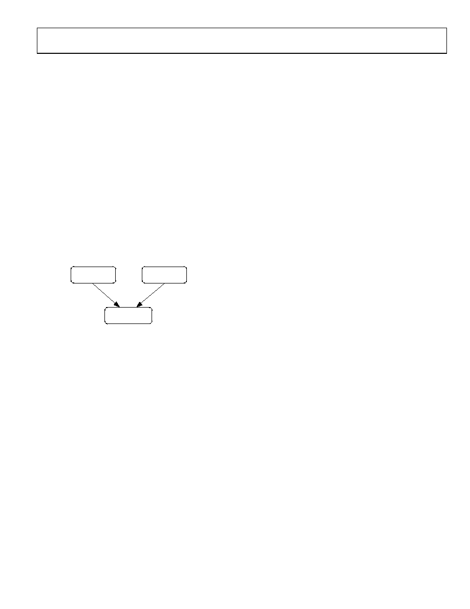
This technology is basically an outgrowth of EPROM technol-
ogy and was developed through the late 1980s. Flash/EE memory
takes the flexible in-circuit reprogrammable features of EEPROM
and combines them with the space efficient/density features of
EPROM (see Figure 47).
Because Flash/EE technology is based on a single transistor cell
architecture, a Flash memory array, like EPROM, can be imple-
mented to achieve the space efficiencies or memory densities
required by a given design. Like EEPROM, Flash memory can
be programmed in-system at a byte level, although it must first
be erased, the erase being performed in page blocks. Thus, Flash
memory is often and more correctly referred to as Flash/EE
memory.
FLASH/EE MEMORY
TECHNOLOGY
SPACE EFFICIENT/
DENSITY
IN-CIRCUIT
REPROGRAMMABLE
EPROM
TECHNOLOGY
EEPROM
TECHNOLOGY
02987-
036
Figure 47. Flash/EE Memory Development
Overall, Flash/EE memory represents a step closer to the
ideal memory device that includes nonvolatility, in-circuit
programmability, high density, and low cost. Incorporated in
the ADuC832, Flash/EE memory technology allows the user
to update program code space in-circuit, without the need to
replace one-time programmable (OTP) devices at remote
operating nodes.
FLASH/EE MEMORY AND THE ADUC832
The ADuC832 provides two arrays of Flash/EE memory for
user applications. There are 62 kB of Flash/EE program space
provided on chip to facilitate code execution without any
external discrete ROM device requirements. The program
memory can be programmed in-circuit using the serial down-
load mode provided, using conventional third party memory
programmers, or via a user defined protocol that can configure
it as data if required.
A 4 kB Flash/EE data memory space is also provided on chip.
This can be used as a general-purpose nonvolatile scratchpad
area. User access to this area is via a group of six SFRs. This
space can be programmed at the byte level, although it must
first be erased in 4-byte pages.
ADUC832 FLASH/EE MEMORY RELIABILITY
The Flash/EE program and data memory arrays on the
ADuC832 are fully qualified for two key Flash/EE memory
characteristics, namely Flash/EE memory cycling endurance
and Flash/EE memory data retention.
Endurance quantifies the ability of the Flash/EE memory to be
cycled through many program, read, and erase cycles. In real
terms, a single Flash/EE memory endurance cycle is composed
of the following four independent, sequential events:
Initial page erase sequence
Read/verify sequence
Byte program sequence
Second read/verify sequence
In reliability qualification, every byte in both the program and
data Flash/EE memory is cycled from 00H to FFH until a first
fail is recorded, signifying the endurance limit of the on-chip
Flash/EE memory.
As indicated in the Specifications section, the ADuC832 Flash/
EE memory endurance qualification has been carried out in
accordance with JEDEC Specification A117 over the industrial
temperature range of 40°C to +25°C and +85°C to +125°C. The
results allow the specification of a minimum endurance value
over supply and temperature of 100,000 cycles, with an endur-
ance value of 700,000 cycles being typical of operation at 25°C.
Retention quantifies the ability of the Flash/EE memory to
retain its programmed data over time. Again, the ADuC832 has
been qualified in accordance with the formal JEDEC retention
lifetime specification (A117) at a specific junction temperature
(TJ = 55°C). As part of this qualification procedure, the Flash/
EE memory is cycled to its specified endurance limit described
previously, before data retention is characterized. This means
that the Flash/EE memory is guaranteed to retain its data for its
full specified retention lifetime every time the Flash/EE memory is
reprogrammed. It should also be noted that retention lifetime,
based on an activation energy of 0.6 eV, derates with TJ, as shown
相关PDF资料 |
PDF描述 |
|---|---|
| ADUC834BCPZ-REEL | IC MCU 62K FLASH ADC/DAC 56LFCSP |
| ADUC836BCPZ | IC MCU 62K FLASH ADC/DAC 56LFCSP |
| ADUC843BSZ62-5 | IC ADC 12BIT W/FLASH MCU 52-MQFP |
| ADUC845BCPZ62-5 | IC FLASH MCU W/24BIT ADC 56-CSP |
| ADUC847BCPZ62-5 | IC MCU FLASH W/24BIT ADC 56-CSP |
相关代理商/技术参数 |
参数描述 |
|---|---|
| ADUC832QS-U1 | 制造商:Analog Devices 功能描述:EVAL KIT - Bulk |
| ADUC834 | 制造商:AD 制造商全称:Analog Devices 功能描述:MicroConverter, Dual 16-Bit/24-Bit ADCs with Embedded 62 kB Flash MCU |
| ADUC834_02 | 制造商:AD 制造商全称:Analog Devices 功能描述:MicroConverter, Dual 16-Bit/24-Bit ADCs with Embedded 62 kB Flash MCU |
| ADUC834BCP | 制造商:Rochester Electronics LLC 功能描述:8BIT CISC 62KB FLASH 12.58MHZ 3.3/5V 56LFCSP - Bulk 制造商:Analog Devices 功能描述: |
| ADUC834BCPZ | 功能描述:IC MCU 62K FLASH ADC/DAC 56LFCSP RoHS:是 类别:集成电路 (IC) >> 嵌入式 - 微控制器, 系列:MicroConverter® ADuC8xx 标准包装:250 系列:LPC11Uxx 核心处理器:ARM? Cortex?-M0 芯体尺寸:32-位 速度:50MHz 连通性:I²C,Microwire,SPI,SSI,SSP,UART/USART,USB 外围设备:欠压检测/复位,POR,WDT 输入/输出数:40 程序存储器容量:96KB(96K x 8) 程序存储器类型:闪存 EEPROM 大小:4K x 8 RAM 容量:10K x 8 电压 - 电源 (Vcc/Vdd):1.8 V ~ 3.6 V 数据转换器:A/D 8x10b 振荡器型:内部 工作温度:-40°C ~ 85°C 封装/外壳:48-LQFP 包装:托盘 其它名称:568-9587 |
发布紧急采购,3分钟左右您将得到回复。