- 您现在的位置:买卖IC网 > PDF目录1900 > ADUC832BSZ-REEL (Analog Devices Inc)IC MCU 62K FLASH ADC/DAC 52MQFP PDF资料下载
参数资料
| 型号: | ADUC832BSZ-REEL |
| 厂商: | Analog Devices Inc |
| 文件页数: | 82/92页 |
| 文件大小: | 0K |
| 描述: | IC MCU 62K FLASH ADC/DAC 52MQFP |
| 标准包装: | 800 |
| 系列: | MicroConverter® ADuC8xx |
| 核心处理器: | 8052 |
| 芯体尺寸: | 8-位 |
| 速度: | 16MHz |
| 连通性: | EBI/EMI,I²C,SPI,UART/USART |
| 外围设备: | PSM,温度传感器,WDT |
| 输入/输出数: | 34 |
| 程序存储器容量: | 62KB(62K x 8) |
| 程序存储器类型: | 闪存 |
| EEPROM 大小: | 4K x 8 |
| RAM 容量: | 2.25K x 8 |
| 电压 - 电源 (Vcc/Vdd): | 2.7 V ~ 5.5 V |
| 数据转换器: | A/D 8x12b,D/A 2x12b |
| 振荡器型: | 内部 |
| 工作温度: | -40°C ~ 125°C |
| 封装/外壳: | 52-QFP |
| 包装: | 带卷 (TR) |
第1页第2页第3页第4页第5页第6页第7页第8页第9页第10页第11页第12页第13页第14页第15页第16页第17页第18页第19页第20页第21页第22页第23页第24页第25页第26页第27页第28页第29页第30页第31页第32页第33页第34页第35页第36页第37页第38页第39页第40页第41页第42页第43页第44页第45页第46页第47页第48页第49页第50页第51页第52页第53页第54页第55页第56页第57页第58页第59页第60页第61页第62页第63页第64页第65页第66页第67页第68页第69页第70页第71页第72页第73页第74页第75页第76页第77页第78页第79页第80页第81页当前第82页第83页第84页第85页第86页第87页第88页第89页第90页第91页第92页
Data Sheet
ADuC832
Rev. B | Page 83 of 92
LATCH
SRAM
A8 TO A15
A0 TO A7
D0 TO D7
(DATA)
ADuC832
P2
ALE
P0
0
298
7-
0
76
RD
WR
OE
WE
Figure 88. External Data Memory Interface (64 kB Address Space)
If access to more than 64 kB of RAM is desired, a feature unique
to the ADuC832 allows addressing up to 16 MB of external
RAM simply by adding an additional latch, as illustrated in
LATCH
ADuC832
RD
P2
ALE
P0
WR
LATCH
SRAM
OE
A8 TO A15
A0 TO A7
D0 TO D7
(DATA)
WE
A16 TO A23
0
29
87
-07
7
Figure 89. External Data Memory Interface (16 MB Address Space)
In either implementation, Port 0 (P0) serves as a multiplexed
address/data bus. It emits the low byte of the data pointer (DPL)
as an address, which is latched by a pulse of ALE prior to data
being placed on the bus by the ADuC832 (write operation) or
the SRAM (read operation). Port 2 (P2) provides the data
pointer page byte (DPP) to be latched by ALE, followed by the
data pointer high byte (DPH). If no latch is connected to P2,
DPP is ignored by the SRAM, and the 8051 standard of 64 kB
external data memory access is maintained.
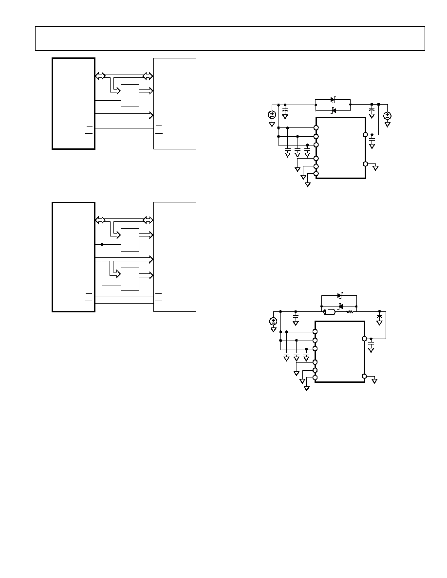
POWER SUPPLIES
The ADuC832 operational power supply voltage range is 2.7 V
to 5.25 V. Although the guaranteed data sheet specifications are
given only for power supplies within 2.7 V to 3.6 V or 10% of
the nominal 5 V level, the chip functions equally well at any
power supply level between 2.7 V and 5.5 V.
Note that Figure 90 and Figure 91 refer to the MQFP package.
For the LFCSP package, connect the extra DVDD, DGND, AVDD,
and AGND in the same manner.
Separate analog and digital power supply pins (AVDD and DVDD,
respectively) allow AVDD to be relatively free of noisy digital signals
often present on the system DVDD line. However, though AVDD
and DVDD can be powered from two separate supplies if desired,
they must remain within 0.3 V of one another at all times to
avoid damaging the chip (as per the Absolute Maximum Ratings
section). Therefore, it is recommended that, unless AVDD and
DVDD are connected directly together, back-to-back Schottky
diodes be connected between them as shown in Figure 90.
DVDD
ADuC832
AGND
AVDD
0.1F
10F
ANALOG SUPPLY
10F
DGND
DIGITAL SUPPLY
02
98
7-
0
78
Figure 90. External Dual-Supply Connections
As an alternative to providing two separate power supplies,
the user can keep AVDD quiet by placing a small series resistor
and/or ferrite bead between it and DVDD, and then decoupling
AVDD separately to ground. An example of this configuration is
shown in Figure 91. With this configuration, other analog circuitry
(such as op amps and voltage reference) can be powered from
the AVDD supply line as well. The user should still include back-
to-back Schottky diodes between AVDD and DVDD to protect
from power-up and power-down transient conditions that may
separate the two supply voltages momentarily.
10F
DVDD
ADuC832
AGND
DGND
0.1F
DIGITAL SUPPLY
1.6
BEAD
AVDD
0
29
87
-07
9
Figure 91. External Single-Supply Connections
Note that, in both Figure 90 and Figure 91, a large value (10 μF)
reservoir capacitor is connected to DVDD and a separate 10 μF
capacitor is connected to AVDD. Also, local small-value (0.1 μF)
capacitors are located at each AVDD pin of the chip. As per stan-
dard design practice, be sure to include all of these capacitors,
and ensure that the smaller capacitors are close to each AVDD
pin with trace lengths as short as possible. Connect the ground
terminal of each of these capacitors directly to the underlying
ground plane. Finally, it should also be noted that, at all times,
the analog and digital ground pins on the ADuC832 must be
referenced to the same system ground reference point.
相关PDF资料 |
PDF描述 |
|---|---|
| ADUC834BCPZ-REEL | IC MCU 62K FLASH ADC/DAC 56LFCSP |
| ADUC836BCPZ | IC MCU 62K FLASH ADC/DAC 56LFCSP |
| ADUC843BSZ62-5 | IC ADC 12BIT W/FLASH MCU 52-MQFP |
| ADUC845BCPZ62-5 | IC FLASH MCU W/24BIT ADC 56-CSP |
| ADUC847BCPZ62-5 | IC MCU FLASH W/24BIT ADC 56-CSP |
相关代理商/技术参数 |
参数描述 |
|---|---|
| ADUC832QS-U1 | 制造商:Analog Devices 功能描述:EVAL KIT - Bulk |
| ADUC834 | 制造商:AD 制造商全称:Analog Devices 功能描述:MicroConverter, Dual 16-Bit/24-Bit ADCs with Embedded 62 kB Flash MCU |
| ADUC834_02 | 制造商:AD 制造商全称:Analog Devices 功能描述:MicroConverter, Dual 16-Bit/24-Bit ADCs with Embedded 62 kB Flash MCU |
| ADUC834BCP | 制造商:Rochester Electronics LLC 功能描述:8BIT CISC 62KB FLASH 12.58MHZ 3.3/5V 56LFCSP - Bulk 制造商:Analog Devices 功能描述: |
| ADUC834BCPZ | 功能描述:IC MCU 62K FLASH ADC/DAC 56LFCSP RoHS:是 类别:集成电路 (IC) >> 嵌入式 - 微控制器, 系列:MicroConverter® ADuC8xx 标准包装:250 系列:LPC11Uxx 核心处理器:ARM? Cortex?-M0 芯体尺寸:32-位 速度:50MHz 连通性:I²C,Microwire,SPI,SSI,SSP,UART/USART,USB 外围设备:欠压检测/复位,POR,WDT 输入/输出数:40 程序存储器容量:96KB(96K x 8) 程序存储器类型:闪存 EEPROM 大小:4K x 8 RAM 容量:10K x 8 电压 - 电源 (Vcc/Vdd):1.8 V ~ 3.6 V 数据转换器:A/D 8x10b 振荡器型:内部 工作温度:-40°C ~ 85°C 封装/外壳:48-LQFP 包装:托盘 其它名称:568-9587 |
发布紧急采购,3分钟左右您将得到回复。