- 您现在的位置:买卖IC网 > PDF目录11720 > ADUC834BCPZ (Analog Devices Inc)IC MCU 62K FLASH ADC/DAC 56LFCSP PDF资料下载
参数资料
| 型号: | ADUC834BCPZ |
| 厂商: | Analog Devices Inc |
| 文件页数: | 53/80页 |
| 文件大小: | 0K |
| 描述: | IC MCU 62K FLASH ADC/DAC 56LFCSP |
| 标准包装: | 1 |
| 系列: | MicroConverter® ADuC8xx |
| 核心处理器: | 8052 |
| 芯体尺寸: | 8-位 |
| 速度: | 12.58MHz |
| 连通性: | EBI/EMI,I²C,SPI,UART/USART |
| 外围设备: | POR,PSM,PWM,温度传感器,WDT |
| 输入/输出数: | 34 |
| 程序存储器容量: | 62KB(62K x 8) |
| 程序存储器类型: | 闪存 |
| EEPROM 大小: | 4K x 8 |
| RAM 容量: | 2.25K x 8 |
| 电压 - 电源 (Vcc/Vdd): | 2.7 V ~ 5.25 V |
| 数据转换器: | A/D 3x16b,4x24b; D/A 1x12b |
| 振荡器型: | 内部 |
| 工作温度: | -40°C ~ 85°C |
| 封装/外壳: | 56-VFQFN 裸露焊盘,CSP |
| 包装: | 托盘 |
第1页第2页第3页第4页第5页第6页第7页第8页第9页第10页第11页第12页第13页第14页第15页第16页第17页第18页第19页第20页第21页第22页第23页第24页第25页第26页第27页第28页第29页第30页第31页第32页第33页第34页第35页第36页第37页第38页第39页第40页第41页第42页第43页第44页第45页第46页第47页第48页第49页第50页第51页第52页当前第53页第54页第55页第56页第57页第58页第59页第60页第61页第62页第63页第64页第65页第66页第67页第68页第69页第70页第71页第72页第73页第74页第75页第76页第77页第78页第79页第80页
REV. A
ADuC834
–57–
UART SERIAL INTERFACE
The serial port is full duplex, meaning it can transmit and
receive simultaneously. It is also receive-buffered, meaning it
can commence reception of a second byte before a previously
received byte has been read from the receive register. However,
if the first byte still has not been read by the time reception of
the second byte is complete, the first byte will be lost. The
physical interface to the serial data network is via Pins
RxD(P3.0) and TxD(P3.1), while the SFR interface to the UART
comprises the following registers:
SBUF
The serial port receive and transmit registers are both accessed
through the SBUF SFR (SFR address = 99H). Writing to SBUF
loads the transmit register and reading SBUF accesses a physically
separate receive register.
SCON
UART Serial Port Control Registers
SFR Address
98H
Power-On Default Value
00H
Bit Addressable
Yes
Table XXX. SCON SFR Bit Designations
Bit
Name
Description
7
SM0
UART Serial Mode Select Bits.
6
SM1
These bits select the Serial Port operating mode as follows:
SM0
SM1
Selected Operating Mode
00
Mode 0: Shift Register, fixed baud rate (fCORE/12)
01
Mode 1: 8-bit UART, variable baud rate
10
Mode 2: 9-bit UART, fixed baud rate (fCORE/64) or (fCORE/32)
11
Mode 3: 9-bit UART, variable baud rate
5
SM2
Multiprocessor Communication Enable Bit.
Enables multiprocessor communication in Modes 2 and 3. In Mode 0, SM2 should be cleared. In
Mode 1, if SM2 is set, RI will not be activated if a valid stop bit was not received. If SM2 is cleared,
RI will be set as soon as the byte of data has been received. In Modes 2 or 3, if SM2 is set, RI will not be
activated if the received ninth data bit in RB8 is 0. If SM2 is cleared, RI will be set as soon as the byte
of data has been received.
4
REN
Serial Port Receive Enable Bit.
Set by user software to enable serial port reception.
Cleared by user software to disable serial port reception.
3TB8
Serial Port Transmit (Bit 9).
The data loaded into TB8 will be the ninth data bit that will be transmitted in Modes 2 and 3.
2
RB8
Serial Port Receiver Bit 9.
The ninth data bit received in Modes 2 and 3 is latched into RB8. For Mode 1, the stop bit is latched into RB8.
1TI
Serial Port Transmit Interrupt Flag.
Set by hardware at the end of the eighth bit in Mode 0, or at the beginning of the stop bit in
Modes 1, 2, and 3.
TI must be cleared by user software.
0RI
Serial Port Receive Interrupt Flag.
Set by hardware at the end of the eighth bit in Mode 0, or halfway through the stop bit in
Modes 1, 2, and 3.
RI must be cleared by software.
UART OPERATING MODES
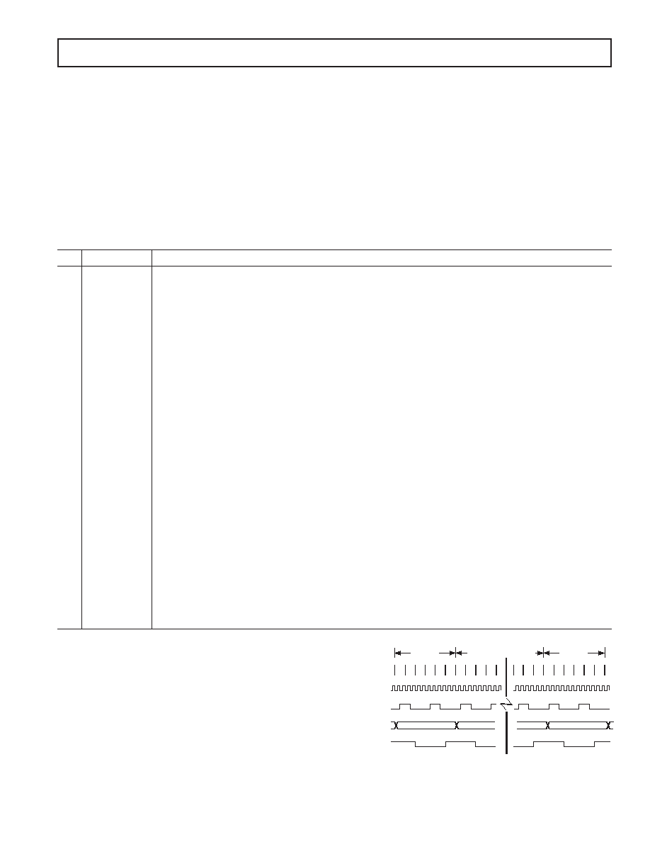
Mode 0: 8-Bit Shift Register Mode
Mode 0 is selected by clearing both the SM0 and SM1 bits in the
SFR SCON. Serial data enters and exits through RxD. TxD outputs
the shift clock. Eight data bits are transmitted or received. Trans-
mission is initiated by any instruction that writes to SBUF. The
data is shifted out of the RxD line. The 8 bits are transmitted
with the least-significant bit (LSB) first, as shown in Figure 54.
Reception is initiated when the Receive Enable bit (REN) is
1 and the Receive Interrupt bit (RI) is 0. When RI is cleared,
the data is clocked into the RxD line and the clock pulses are
output from the TxD line.
CORE
CLK
ALE
RxD
(DATA OUT)
TxD
(SHIFT CLOCK)
DATA BIT 0
DATA BIT 1
DATA BIT 6
DATA BIT 7
S6
S5
S4
S3
S2
S1
S6
S5
S4
S3
S2
S1
S6
S5
S4
S3
S2
S1
MACHINE
CYCLE 8
MACHINE
CYCLE 7
MACHINE
CYCLE 2
MACHINE
CYCLE 1
Figure 54. UART Serial Port Transmission, Mode 0
相关PDF资料 |
PDF描述 |
|---|---|
| ADUC845BSZ62-3 | IC MCU FLASH 24BIT ADC 52MQFP |
| ADUC845BSZ62-5 | IC FLASH MCU W/24BIT ADC 52-MQFP |
| PI7C8150BMAIE | IC PCI-PCI BRIDGE ASYNC 208-FQFP |
| VE-B7J-IX-F4 | CONVERTER MOD DC/DC 36V 75W |
| AT89LP51-20JU | MCU 8051 4K FLASH 20MHZ |
相关代理商/技术参数 |
参数描述 |
|---|---|
| ADUC834BCPZ-REEL | 功能描述:IC MCU 62K FLASH ADC/DAC 56LFCSP RoHS:是 类别:集成电路 (IC) >> 嵌入式 - 微控制器, 系列:MicroConverter® ADuC8xx 标准包装:38 系列:Encore!® XP® 核心处理器:eZ8 芯体尺寸:8-位 速度:5MHz 连通性:IrDA,UART/USART 外围设备:欠压检测/复位,LED,POR,PWM,WDT 输入/输出数:16 程序存储器容量:4KB(4K x 8) 程序存储器类型:闪存 EEPROM 大小:- RAM 容量:1K x 8 电压 - 电源 (Vcc/Vdd):2.7 V ~ 3.6 V 数据转换器:- 振荡器型:内部 工作温度:-40°C ~ 105°C 封装/外壳:20-SOIC(0.295",7.50mm 宽) 包装:管件 其它名称:269-4116Z8F0413SH005EG-ND |
| ADUC834BS | 制造商:Analog Devices 功能描述:MCU 8-bit ADuC8xx 8052 CISC 62KB Flash 3.3V/5V 52-Pin MQFP 制造商:Rochester Electronics LLC 功能描述:8BIT CISC 62KB FLASH 12.58MHZ 3.3/5V 52MQFP - Bulk 制造商:Analog Devices 功能描述:8BIT MCU +24/16BIT ADC SMD MQFP52 |
| ADUC834BSZ | 功能描述:IC ADC DUAL16/24BIT W/MCU 52MQFP RoHS:是 类别:集成电路 (IC) >> 嵌入式 - 微控制器, 系列:MicroConverter® ADuC8xx 标准包装:250 系列:56F8xxx 核心处理器:56800E 芯体尺寸:16-位 速度:60MHz 连通性:CAN,SCI,SPI 外围设备:POR,PWM,温度传感器,WDT 输入/输出数:21 程序存储器容量:40KB(20K x 16) 程序存储器类型:闪存 EEPROM 大小:- RAM 容量:6K x 16 电压 - 电源 (Vcc/Vdd):2.25 V ~ 3.6 V 数据转换器:A/D 6x12b 振荡器型:内部 工作温度:-40°C ~ 125°C 封装/外壳:48-LQFP 包装:托盘 配用:MC56F8323EVME-ND - BOARD EVALUATION MC56F8323 |
| ADUC836 | 制造商:AD 制造商全称:Analog Devices 功能描述:MicroConverter, Dual 16-Bit-ADCs with Embedded 62 kB Flash MCU |
| ADUC836_02 | 制造商:AD 制造商全称:Analog Devices 功能描述:MicroConverter, Dual 16-Bit ADCs with Embedded 62 kB Flash MCU |
发布紧急采购,3分钟左右您将得到回复。