- 您现在的位置:买卖IC网 > PDF目录11197 > ADUC847BCPZ62-3 (Analog Devices Inc)IC MCU FLASH 24BIT ADC 56LFCSP PDF资料下载
参数资料
| 型号: | ADUC847BCPZ62-3 |
| 厂商: | Analog Devices Inc |
| 文件页数: | 33/108页 |
| 文件大小: | 0K |
| 描述: | IC MCU FLASH 24BIT ADC 56LFCSP |
| 标准包装: | 1 |
| 系列: | MicroConverter® ADuC8xx |
| 核心处理器: | 8052 |
| 芯体尺寸: | 8-位 |
| 速度: | 12.58MHz |
| 连通性: | I²C,SPI,UART/USART |
| 外围设备: | POR,PSM,PWM,温度传感器,WDT |
| 输入/输出数: | 34 |
| 程序存储器容量: | 62KB(62K x 8) |
| 程序存储器类型: | 闪存 |
| EEPROM 大小: | 4K x 8 |
| RAM 容量: | 2.25K x 8 |
| 电压 - 电源 (Vcc/Vdd): | 2.7 V ~ 3.6 V |
| 数据转换器: | A/D 10x24b; D/A 1x12b,2x16b |
| 振荡器型: | 内部 |
| 工作温度: | -40°C ~ 85°C |
| 封装/外壳: | 56-VFQFN 裸露焊盘,CSP |
| 包装: | 托盘 |
| 配用: | EVAL-ADUC847QSZ-ND - KIT DEV QUICK START FOR ADUC847 |
第1页第2页第3页第4页第5页第6页第7页第8页第9页第10页第11页第12页第13页第14页第15页第16页第17页第18页第19页第20页第21页第22页第23页第24页第25页第26页第27页第28页第29页第30页第31页第32页当前第33页第34页第35页第36页第37页第38页第39页第40页第41页第42页第43页第44页第45页第46页第47页第48页第49页第50页第51页第52页第53页第54页第55页第56页第57页第58页第59页第60页第61页第62页第63页第64页第65页第66页第67页第68页第69页第70页第71页第72页第73页第74页第75页第76页第77页第78页第79页第80页第81页第82页第83页第84页第85页第86页第87页第88页第89页第90页第91页第92页第93页第94页第95页第96页第97页第98页第99页第100页第101页第102页第103页第104页第105页第106页第107页第108页
ADuC845/ADuC847/ADuC848
Data Sheet
Rev. C | Page 30 of 108
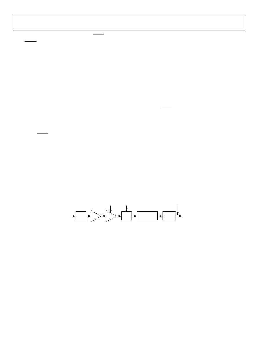
Signal Chain Overview with Chop Disabled (CHOP = 1)
With CHOP = 1, chop is disabled and the available output rates
vary from 16.06 Hz to 1.365 kHz. The range of applicable SF
words is from 3 to 255. When switching between channels with
chop disabled, the channel throughput rate is higher than when
chop is enabled. The drawback with chop disabled is that the
drift performance is degraded and offset calibration is required
following a gain range change or significant temperature
change. A block diagram of the ADC input channel with chop
disabled is shown in Figure 15.
The signal chain includes a multiplex or buffer, PGA, Σ-Δ
modulator, and digital filter. The modulator bit stream is
applied to a Sinc3 filter. Programming the Sinc3 decimation
factor is restricted to an 8-bit register SF; the actual decimation
factor is the register value times 8. The decimated output rate
from the Sinc3 filter (and the ADC conversion rate) is therefore
MOD
ADC
f
SF
f
×
=
8
1
where:
fADC is the ADC conversion rate.
SF is the decimal equivalent of the word loaded to the filter
register, valid range is from 3 to 255.
fMOD is the modulator sampling rate of 32.768 kHz.
The settling time to a step input is governed by the digital filter.
A synchronized step change requires a settling time of three
times the programmed update rate; a channel change can be
treated as a synchronized step change. This is one conversion
longer than the case for chop enabled. However, because the
ADC throughput is three times faster with chop disabled than it
is with chop enabled, the actual time to a settled ADC output is
significantly less also. This means that following a synchronized
step change, the ADC requires three conversions (note: data is
not output following a synchronized ADC change until data has
settled) before the result accurately reflects the new input
voltage.
ADC
SETTLE
t
f
t
×
=
3
An unsynchronized step change requires four conversions to
accurately reflect the new analog input at its output. Note that
with an unsynchronized change the ADC continues to output
data and so the user must take unsettled outputs into account.
Again, this is one conversion longer than with chop enabled, but
because the ADC throughput with chop disabled is faster than
with chop enabled, the actual time taken to obtain a settled
ADC output is less.
The allowable range for SF is 3 to 255 with a default of 69 (45H).
The corresponding conversion rates, rms, and peak-to-peak
noise performances are shown in Table 14, Table 15, Table 16,
and Table 17. Note that the conversion time increases by 0.244 ms
for each increment in SF.
SINC3 FILTER
PGA
8
× SF
S-D
MOD
FADC
DIGITAL
OUTPUT
ANALOG
INPUT
MUX
BUF
FMOD
FIN
04741-015
Figure 15. Block Diagram of ADC Input Channel with Chop Disabled
相关PDF资料 |
PDF描述 |
|---|---|
| AT91SAM7XC256B-CU | MCU ARM 256K HS FLASH 100-TFBGA |
| EP7312M-CBZ | IC ARM720T MCU 74MHZ 256-PBGA |
| EP9301-IQZ | IC ARM920T MCU 166MHZ 208-LQFP |
| AT91SAM7X256C-CU | IC MCU 32BIT 256KB FLSH 100TFBGA |
| ADUC845BSZ8-3 | IC MCU FLASH 24BIT ADC 52MQFP |
相关代理商/技术参数 |
参数描述 |
|---|---|
| ADUC847BCPZ62-5 | 功能描述:IC MCU FLASH W/24BIT ADC 56-CSP RoHS:是 类别:集成电路 (IC) >> 嵌入式 - 微控制器, 系列:MicroConverter® ADuC8xx 标准包装:38 系列:Encore!® XP® 核心处理器:eZ8 芯体尺寸:8-位 速度:5MHz 连通性:IrDA,UART/USART 外围设备:欠压检测/复位,LED,POR,PWM,WDT 输入/输出数:16 程序存储器容量:4KB(4K x 8) 程序存储器类型:闪存 EEPROM 大小:- RAM 容量:1K x 8 电压 - 电源 (Vcc/Vdd):2.7 V ~ 3.6 V 数据转换器:- 振荡器型:内部 工作温度:-40°C ~ 105°C 封装/外壳:20-SOIC(0.295",7.50mm 宽) 包装:管件 其它名称:269-4116Z8F0413SH005EG-ND |
| ADUC847BCPZ8-3 | 功能描述:IC MCU FLASH W/24BIT ADC 56-CSP RoHS:是 类别:集成电路 (IC) >> 嵌入式 - 微控制器, 系列:MicroConverter® ADuC8xx 标准包装:38 系列:Encore!® XP® 核心处理器:eZ8 芯体尺寸:8-位 速度:5MHz 连通性:IrDA,UART/USART 外围设备:欠压检测/复位,LED,POR,PWM,WDT 输入/输出数:16 程序存储器容量:4KB(4K x 8) 程序存储器类型:闪存 EEPROM 大小:- RAM 容量:1K x 8 电压 - 电源 (Vcc/Vdd):2.7 V ~ 3.6 V 数据转换器:- 振荡器型:内部 工作温度:-40°C ~ 105°C 封装/外壳:20-SOIC(0.295",7.50mm 宽) 包装:管件 其它名称:269-4116Z8F0413SH005EG-ND |
| ADUC847BCPZ8-5 | 功能描述:IC MCU FLASH W/24BIT ADC 56-CSP RoHS:是 类别:集成电路 (IC) >> 嵌入式 - 微控制器, 系列:MicroConverter® ADuC8xx 标准包装:38 系列:Encore!® XP® 核心处理器:eZ8 芯体尺寸:8-位 速度:5MHz 连通性:IrDA,UART/USART 外围设备:欠压检测/复位,LED,POR,PWM,WDT 输入/输出数:16 程序存储器容量:4KB(4K x 8) 程序存储器类型:闪存 EEPROM 大小:- RAM 容量:1K x 8 电压 - 电源 (Vcc/Vdd):2.7 V ~ 3.6 V 数据转换器:- 振荡器型:内部 工作温度:-40°C ~ 105°C 封装/外壳:20-SOIC(0.295",7.50mm 宽) 包装:管件 其它名称:269-4116Z8F0413SH005EG-ND |
| ADUC847BS32-3 | 制造商:Analog Devices 功能描述:MCU 8-Bit ADuC8xx 8052 CISC 62KB Flash 3.3V/5V 52-Pin MQFP 制造商:Rochester Electronics LLC 功能描述:8BIT CISC 62KB FLASH 12.85MHZ 3.3V 52MQFP - Bulk |
| ADUC847BS32-5 | 制造商:Analog Devices 功能描述:MCU 8-Bit ADuC8xx 8052 CISC 62KB Flash 3.3V/5V 52-Pin MQFP 制造商:Rochester Electronics LLC 功能描述: |
发布紧急采购,3分钟左右您将得到回复。