- 您现在的位置:买卖IC网 > PDF目录11197 > ADUC847BCPZ62-3 (Analog Devices Inc)IC MCU FLASH 24BIT ADC 56LFCSP PDF资料下载
参数资料
| 型号: | ADUC847BCPZ62-3 |
| 厂商: | Analog Devices Inc |
| 文件页数: | 80/108页 |
| 文件大小: | 0K |
| 描述: | IC MCU FLASH 24BIT ADC 56LFCSP |
| 标准包装: | 1 |
| 系列: | MicroConverter® ADuC8xx |
| 核心处理器: | 8052 |
| 芯体尺寸: | 8-位 |
| 速度: | 12.58MHz |
| 连通性: | I²C,SPI,UART/USART |
| 外围设备: | POR,PSM,PWM,温度传感器,WDT |
| 输入/输出数: | 34 |
| 程序存储器容量: | 62KB(62K x 8) |
| 程序存储器类型: | 闪存 |
| EEPROM 大小: | 4K x 8 |
| RAM 容量: | 2.25K x 8 |
| 电压 - 电源 (Vcc/Vdd): | 2.7 V ~ 3.6 V |
| 数据转换器: | A/D 10x24b; D/A 1x12b,2x16b |
| 振荡器型: | 内部 |
| 工作温度: | -40°C ~ 85°C |
| 封装/外壳: | 56-VFQFN 裸露焊盘,CSP |
| 包装: | 托盘 |
| 配用: | EVAL-ADUC847QSZ-ND - KIT DEV QUICK START FOR ADUC847 |
第1页第2页第3页第4页第5页第6页第7页第8页第9页第10页第11页第12页第13页第14页第15页第16页第17页第18页第19页第20页第21页第22页第23页第24页第25页第26页第27页第28页第29页第30页第31页第32页第33页第34页第35页第36页第37页第38页第39页第40页第41页第42页第43页第44页第45页第46页第47页第48页第49页第50页第51页第52页第53页第54页第55页第56页第57页第58页第59页第60页第61页第62页第63页第64页第65页第66页第67页第68页第69页第70页第71页第72页第73页第74页第75页第76页第77页第78页第79页当前第80页第81页第82页第83页第84页第85页第86页第87页第88页第89页第90页第91页第92页第93页第94页第95页第96页第97页第98页第99页第100页第101页第102页第103页第104页第105页第106页第107页第108页
Data Sheet
ADuC845/ADuC847/ADuC848
Rev. C | Page 73 of 108
8052-COMPATIBLE ON-CHIP PERIPHERALS
This section gives a brief overview of the various secondary
peripheral circuits that are available to the user on-chip. These
features are mostly 8052-compatible (with a few additional
features) and are controlled via standard 8052 SFR bit definitions.
Parallel I/O
The ADuC845/ADuC847/ADuC848 use four input/output
ports to exchange data with external devices. In addition to
performing general-purpose I/O, some are capable of external
memory operations, while others are multiplexed with alternate
functions for the peripheral functions available on-chip. In
general, when a peripheral is enabled, that pin cannot be used
as a general-purpose I/O pin.
Port 0
Port 0 is an 8-bit open-drain bidirectional I/O port that is
directly controlled via the Port 0 SFR (80H). Port 0 is also the
multiplexed low-order address and data bus during accesses to
external data memory.
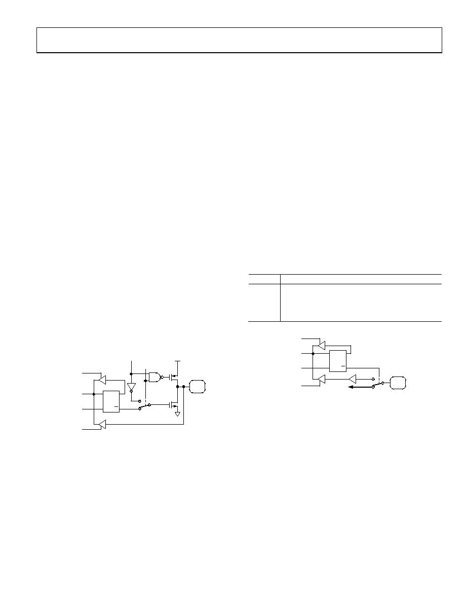
Figure 48 shows a typical bit latch and I/O buffer for a Port 0
pin. The bit latch (one bit in the port’s SFR) is represented as a
Type D flip-flop, which clocks in a value from the internal bus
in response to a write to latch signal from the CPU. The
Q output of the flip-flop is placed on the internal bus in
response to a read latch signal from the CPU. The level of the
port pin itself is placed on the internal bus in response to a read
pin signal from the CPU. Some instructions that read a port
activate the read latch signal, and others activate the read pin
signal. See the Read-Modify-Write Instructions section for
details.
CONTROL
READ
LATCH
INTERNAL
BUS
WRITE
TO LATCH
READ
PIN
D
CL
Q
LATCH
DVDD
ADDR/DATA
P0.x
PIN
04741-048
Figure 48. Port 0 Bit Latch and I/O Buffer
As shown in Figure 48, the output drivers of Port 0 pins are
switchable to an internal ADDR and ADDR/DATA bus by an
internal control signal for use in external memory accesses.
During external memory accesses, the P0 SFR has 1s written to
it; therefore, all its bit latches become 1. When accessing
external memory, the control signal in Figure 48 goes high,
enabling push-pull operation of the output pin from the internal
address or data bus (ADDR/DATA line). Therefore, no external
pull-ups are required on Port 0 for it to access external memory.
In general-purpose I/O port mode, Port 0 pins that have 1s
written to them via the Port 0 SFR are configured as open-drain
and, therefore, float. In this state, Port 0 pins can be used as
high impedance inputs. This is represented in Figure 48 by the
NAND gate whose output remains high as long as the control
signal is low, thereby disabling the top FET. External pull-up
resistors are, therefore, required when Port 0 pins are used as
general-purpose outputs. Port 0 pins with 0s written to them
drive a logic low output voltage (VOL) and are capable of sinking
1.6 mA.
Port 1
Port 1 is also an 8-bit port directly controlled via the P1 SFR
(90H). Port 1 digital output capability is not supported on this
device. Port 1 pins can be configured as digital inputs or analog
inputs. By (power-on) default, these pins are configured as
analog inputs, that is, 1 is written to the corresponding Port 1
register bit. To configure any of these pins as digital inputs, the
user should write a 0 to these port bits to configure the corre-
sponding pin as a high impedance digital input. These pins also
have various secondary functions aside from their analog input
capability, as described in Table 46.
Table 46. Port 1 Alternate Functions
Pin No.
Alternate Function
P1.2
REFIN2+ (second reference input, +’ve)
P1.3
REFIN2 (second reference input, –‘ve)
P1.6
IEXC1 (200 A excitation current source)
P1.7
IEXC2 (200 A excitation current source)
READ
LATCH
INTERNAL
BUS
WRITE
TO LATCH
READ
PIN
D
CL
Q
LATCH
P1.x
PIN
TO ADC
04741-068
Figure 49. Port 1 Bit Latch and I/O Buffer
Port 2
Port 2 is a bidirectional port with internal pull-up resistors
directly controlled via the P2 SFR. Port 2 also emits the middle-
and high-order address bytes during accesses to the 24-bit
external data memory space.
In general-purpose I/O port mode, Port 2 pins that have 1s
written to them are pulled high by the internal pull-ups as
shown in Figure 50 and, in that state, can be used as inputs. As
inputs, Port 2 pins pulled externally low source current because
of the internal pull-up resistors. Port 2 pins with 0s written to
them drive a logic low output voltage (VOL) and are capable of
sinking 1.6 mA.
相关PDF资料 |
PDF描述 |
|---|---|
| AT91SAM7XC256B-CU | MCU ARM 256K HS FLASH 100-TFBGA |
| EP7312M-CBZ | IC ARM720T MCU 74MHZ 256-PBGA |
| EP9301-IQZ | IC ARM920T MCU 166MHZ 208-LQFP |
| AT91SAM7X256C-CU | IC MCU 32BIT 256KB FLSH 100TFBGA |
| ADUC845BSZ8-3 | IC MCU FLASH 24BIT ADC 52MQFP |
相关代理商/技术参数 |
参数描述 |
|---|---|
| ADUC847BCPZ62-5 | 功能描述:IC MCU FLASH W/24BIT ADC 56-CSP RoHS:是 类别:集成电路 (IC) >> 嵌入式 - 微控制器, 系列:MicroConverter® ADuC8xx 标准包装:38 系列:Encore!® XP® 核心处理器:eZ8 芯体尺寸:8-位 速度:5MHz 连通性:IrDA,UART/USART 外围设备:欠压检测/复位,LED,POR,PWM,WDT 输入/输出数:16 程序存储器容量:4KB(4K x 8) 程序存储器类型:闪存 EEPROM 大小:- RAM 容量:1K x 8 电压 - 电源 (Vcc/Vdd):2.7 V ~ 3.6 V 数据转换器:- 振荡器型:内部 工作温度:-40°C ~ 105°C 封装/外壳:20-SOIC(0.295",7.50mm 宽) 包装:管件 其它名称:269-4116Z8F0413SH005EG-ND |
| ADUC847BCPZ8-3 | 功能描述:IC MCU FLASH W/24BIT ADC 56-CSP RoHS:是 类别:集成电路 (IC) >> 嵌入式 - 微控制器, 系列:MicroConverter® ADuC8xx 标准包装:38 系列:Encore!® XP® 核心处理器:eZ8 芯体尺寸:8-位 速度:5MHz 连通性:IrDA,UART/USART 外围设备:欠压检测/复位,LED,POR,PWM,WDT 输入/输出数:16 程序存储器容量:4KB(4K x 8) 程序存储器类型:闪存 EEPROM 大小:- RAM 容量:1K x 8 电压 - 电源 (Vcc/Vdd):2.7 V ~ 3.6 V 数据转换器:- 振荡器型:内部 工作温度:-40°C ~ 105°C 封装/外壳:20-SOIC(0.295",7.50mm 宽) 包装:管件 其它名称:269-4116Z8F0413SH005EG-ND |
| ADUC847BCPZ8-5 | 功能描述:IC MCU FLASH W/24BIT ADC 56-CSP RoHS:是 类别:集成电路 (IC) >> 嵌入式 - 微控制器, 系列:MicroConverter® ADuC8xx 标准包装:38 系列:Encore!® XP® 核心处理器:eZ8 芯体尺寸:8-位 速度:5MHz 连通性:IrDA,UART/USART 外围设备:欠压检测/复位,LED,POR,PWM,WDT 输入/输出数:16 程序存储器容量:4KB(4K x 8) 程序存储器类型:闪存 EEPROM 大小:- RAM 容量:1K x 8 电压 - 电源 (Vcc/Vdd):2.7 V ~ 3.6 V 数据转换器:- 振荡器型:内部 工作温度:-40°C ~ 105°C 封装/外壳:20-SOIC(0.295",7.50mm 宽) 包装:管件 其它名称:269-4116Z8F0413SH005EG-ND |
| ADUC847BS32-3 | 制造商:Analog Devices 功能描述:MCU 8-Bit ADuC8xx 8052 CISC 62KB Flash 3.3V/5V 52-Pin MQFP 制造商:Rochester Electronics LLC 功能描述:8BIT CISC 62KB FLASH 12.85MHZ 3.3V 52MQFP - Bulk |
| ADUC847BS32-5 | 制造商:Analog Devices 功能描述:MCU 8-Bit ADuC8xx 8052 CISC 62KB Flash 3.3V/5V 52-Pin MQFP 制造商:Rochester Electronics LLC 功能描述: |
发布紧急采购,3分钟左右您将得到回复。