- 您现在的位置:买卖IC网 > PDF目录11197 > ADUC847BCPZ62-3 (Analog Devices Inc)IC MCU FLASH 24BIT ADC 56LFCSP PDF资料下载
参数资料
| 型号: | ADUC847BCPZ62-3 |
| 厂商: | Analog Devices Inc |
| 文件页数: | 52/108页 |
| 文件大小: | 0K |
| 描述: | IC MCU FLASH 24BIT ADC 56LFCSP |
| 标准包装: | 1 |
| 系列: | MicroConverter® ADuC8xx |
| 核心处理器: | 8052 |
| 芯体尺寸: | 8-位 |
| 速度: | 12.58MHz |
| 连通性: | I²C,SPI,UART/USART |
| 外围设备: | POR,PSM,PWM,温度传感器,WDT |
| 输入/输出数: | 34 |
| 程序存储器容量: | 62KB(62K x 8) |
| 程序存储器类型: | 闪存 |
| EEPROM 大小: | 4K x 8 |
| RAM 容量: | 2.25K x 8 |
| 电压 - 电源 (Vcc/Vdd): | 2.7 V ~ 3.6 V |
| 数据转换器: | A/D 10x24b; D/A 1x12b,2x16b |
| 振荡器型: | 内部 |
| 工作温度: | -40°C ~ 85°C |
| 封装/外壳: | 56-VFQFN 裸露焊盘,CSP |
| 包装: | 托盘 |
| 配用: | EVAL-ADUC847QSZ-ND - KIT DEV QUICK START FOR ADUC847 |
第1页第2页第3页第4页第5页第6页第7页第8页第9页第10页第11页第12页第13页第14页第15页第16页第17页第18页第19页第20页第21页第22页第23页第24页第25页第26页第27页第28页第29页第30页第31页第32页第33页第34页第35页第36页第37页第38页第39页第40页第41页第42页第43页第44页第45页第46页第47页第48页第49页第50页第51页当前第52页第53页第54页第55页第56页第57页第58页第59页第60页第61页第62页第63页第64页第65页第66页第67页第68页第69页第70页第71页第72页第73页第74页第75页第76页第77页第78页第79页第80页第81页第82页第83页第84页第85页第86页第87页第88页第89页第90页第91页第92页第93页第94页第95页第96页第97页第98页第99页第100页第101页第102页第103页第104页第105页第106页第107页第108页
ADuC845/ADuC847/ADuC848
Data Sheet
Rev. C | Page 48 of 108
NONVOLATILE FLASH/EE MEMORY OVERVIEW
The ADuC845/ADuC847/ADuC848 incorporate Flash/EE
memory technology on-chip to provide the user with nonvolatile,
in-circuit reprogrammable code and data memory space.
Like EEPROM, flash memory can be programmed in-system at
the byte level, although it must first be erased, in page blocks.
Thus, flash memory is often and more correctly referred to as
Flash/EE memory.
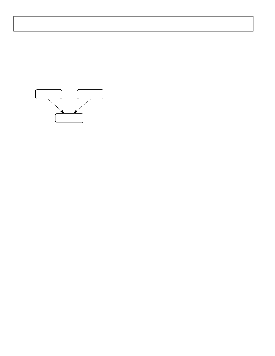
EEPROM
TECHNOLOGY
EPROM
TECHNOLOGY
FLASH/EE MEMORY
TECHNOLOGY
IN-CIRCUIT
REPROGRAMMABLE
SPACE EFFICIENT/
DENSITY
04741-026
Figure 26. Flash/EE Memory Development
Overall, Flash/EE memory represents a step closer to the ideal
memory device that includes nonvolatility, in-circuit program-
mability, high density, and low cost. The Flash/EE memory
technology allows the user to update program code space in-
circuit, without needing to replace onetime programmable
(OTP) devices at remote operating nodes.
Flash/EE Memory on the ADuC845, ADuC847, ADuC848
The ADuC845/ADuC847/ADuC848 provide two arrays of
Flash/EE memory for user applications—up to 62 kbytes of
Flash/EE program space and 4 kbytes of Flash/EE data memory
space. Also, 8-kbyte and 32-kbyte program memory options are
available. All examples and references in this datasheet use the
62-kbyte option; however, similar protocols and procedures are
applicable to the 32-kbyte and 8-kbyte options unless otherwise
noted, provided that the difference in memory size is taken into
account.
The 62 kbytes Flash/EE code space are provided on-chip to
facilitate code execution without any external discrete ROM
device requirements. The program memory can be programmed
in-circuit, using the serial download mode provided, using
conventional third party memory programmers, or via any
user-defined protocol in user download (ULOAD) mode.
The 4-kbyte Flash/EE data memory space can be used as a
general-purpose, nonvolatile scratchpad area. User access to
this area is via a group of seven SFRs. This space can be
programmed at a byte level, although it must first be erased in
4-byte pages.
All the following sections use the 62-kbyte program space as an
example when referring to program and ULOAD mode. For the
64-kbyte part, the ULOAD area takes up the top 6 kbytes of the
program space, that is, from 56 kbytes to 62 kbytes. For the
32-kbyte part, the ULOAD space moves to the top 8 kbytes of the
on-chip program memory, that is., from 24 kbytes to 32 kbytes.
No ULOAD mode is available on the 8-kbyte part since the
bootload area on the 8-kbyte part is 8 kbytes long, so no usable
user program space remains. The kernel still resides in the
protected area from 62 kbytes to 64 kbytes.
Flash/EE Memory Reliability
The Flash/EE program and data memory arrays on the
ADuC845/ADuC847/ADuC848 are fully qualified for two key
Flash/EE memory characteristics: Flash/EE memory cycling
endurance and Flash/EE memory data retention.
Endurance quantifies the ability of the Flash/EE memory to be
cycled through many program, read, and erase cycles. In real
terms, a single endurance cycle is composed of four independent,
sequential events:
1. Initial page erase sequence
2. Read/verify sequence
3. Byte program sequence
4. Second read/verify sequence
In reliability qualification, every byte in both the program and
data Flash/EE memory is cycled from 00H to FFH until a first
fail is recorded, signifying the endurance limit of the on-chip
Flash/EE memory.
As indicated in the Specifications table, the ADuC845/ADuC847/
ADuC848 Flash/EE memory endurance qualification has been
carried out in accordance with JEDEC Specification A117 over
the industrial temperature range of –40°C, +25°C, +85°C, and
+125°C. (The LFCSP package is qualified to +85°C only.) The
results allow the specification of a minimum endurance figure
over supply and temperature of 100,000 cycles, with an endurance
figure of 700,000 cycles being typical of operation at 25°C.
Retention is the ability of the Flash/EE memory to retain its
programmed data over time. Again, the parts have been qualified
in accordance with the formal JEDEC Retention Lifetime Specifi-
cation (A117) at a specific junction temperature (TJ = 55°C). As
part of this qualification procedure, the Flash/EE memory is
cycled to its specified endurance limit described previously,
before data retention is characterized. This means that the
Flash/EE memory is guaranteed to retain its data for its full
specified retention lifetime every time the Flash/EE memory is
reprogrammed. It should also be noted that retention lifetime,
based on an activation energy of 0.6 eV, derates with TJ as shown
相关PDF资料 |
PDF描述 |
|---|---|
| AT91SAM7XC256B-CU | MCU ARM 256K HS FLASH 100-TFBGA |
| EP7312M-CBZ | IC ARM720T MCU 74MHZ 256-PBGA |
| EP9301-IQZ | IC ARM920T MCU 166MHZ 208-LQFP |
| AT91SAM7X256C-CU | IC MCU 32BIT 256KB FLSH 100TFBGA |
| ADUC845BSZ8-3 | IC MCU FLASH 24BIT ADC 52MQFP |
相关代理商/技术参数 |
参数描述 |
|---|---|
| ADUC847BCPZ62-5 | 功能描述:IC MCU FLASH W/24BIT ADC 56-CSP RoHS:是 类别:集成电路 (IC) >> 嵌入式 - 微控制器, 系列:MicroConverter® ADuC8xx 标准包装:38 系列:Encore!® XP® 核心处理器:eZ8 芯体尺寸:8-位 速度:5MHz 连通性:IrDA,UART/USART 外围设备:欠压检测/复位,LED,POR,PWM,WDT 输入/输出数:16 程序存储器容量:4KB(4K x 8) 程序存储器类型:闪存 EEPROM 大小:- RAM 容量:1K x 8 电压 - 电源 (Vcc/Vdd):2.7 V ~ 3.6 V 数据转换器:- 振荡器型:内部 工作温度:-40°C ~ 105°C 封装/外壳:20-SOIC(0.295",7.50mm 宽) 包装:管件 其它名称:269-4116Z8F0413SH005EG-ND |
| ADUC847BCPZ8-3 | 功能描述:IC MCU FLASH W/24BIT ADC 56-CSP RoHS:是 类别:集成电路 (IC) >> 嵌入式 - 微控制器, 系列:MicroConverter® ADuC8xx 标准包装:38 系列:Encore!® XP® 核心处理器:eZ8 芯体尺寸:8-位 速度:5MHz 连通性:IrDA,UART/USART 外围设备:欠压检测/复位,LED,POR,PWM,WDT 输入/输出数:16 程序存储器容量:4KB(4K x 8) 程序存储器类型:闪存 EEPROM 大小:- RAM 容量:1K x 8 电压 - 电源 (Vcc/Vdd):2.7 V ~ 3.6 V 数据转换器:- 振荡器型:内部 工作温度:-40°C ~ 105°C 封装/外壳:20-SOIC(0.295",7.50mm 宽) 包装:管件 其它名称:269-4116Z8F0413SH005EG-ND |
| ADUC847BCPZ8-5 | 功能描述:IC MCU FLASH W/24BIT ADC 56-CSP RoHS:是 类别:集成电路 (IC) >> 嵌入式 - 微控制器, 系列:MicroConverter® ADuC8xx 标准包装:38 系列:Encore!® XP® 核心处理器:eZ8 芯体尺寸:8-位 速度:5MHz 连通性:IrDA,UART/USART 外围设备:欠压检测/复位,LED,POR,PWM,WDT 输入/输出数:16 程序存储器容量:4KB(4K x 8) 程序存储器类型:闪存 EEPROM 大小:- RAM 容量:1K x 8 电压 - 电源 (Vcc/Vdd):2.7 V ~ 3.6 V 数据转换器:- 振荡器型:内部 工作温度:-40°C ~ 105°C 封装/外壳:20-SOIC(0.295",7.50mm 宽) 包装:管件 其它名称:269-4116Z8F0413SH005EG-ND |
| ADUC847BS32-3 | 制造商:Analog Devices 功能描述:MCU 8-Bit ADuC8xx 8052 CISC 62KB Flash 3.3V/5V 52-Pin MQFP 制造商:Rochester Electronics LLC 功能描述:8BIT CISC 62KB FLASH 12.85MHZ 3.3V 52MQFP - Bulk |
| ADUC847BS32-5 | 制造商:Analog Devices 功能描述:MCU 8-Bit ADuC8xx 8052 CISC 62KB Flash 3.3V/5V 52-Pin MQFP 制造商:Rochester Electronics LLC 功能描述: |
发布紧急采购,3分钟左右您将得到回复。