参数资料
| 型号: | ADV3225ACPZ |
| 厂商: | Analog Devices Inc |
| 文件页数: | 22/24页 |
| 文件大小: | 0K |
| 描述: | IC CROSSPOINT SW 16X8 72LFCSP |
| 标准包装: | 1 |
| 功能: | 交叉点开关 |
| 电路: | 1 x 16:8 |
| 电压电源: | 双电源 |
| 电压 - 电源,单路/双路(±): | ±5V |
| 电流 - 电源: | 58mA |
| 工作温度: | -40°C ~ 85°C |
| 安装类型: | 表面贴装 |
| 封装/外壳: | 72-VFQFN 裸露焊盘,CSP |
| 供应商设备封装: | 72-LFCSP-VQ(10x10) |
| 包装: | 托盘 |
ADV3224/ADV3225
Rev. A | Page 7 of 24
ABSOLUTE MAXIMUM RATINGS
Table 5.
Parameter
Rating
Analog Supply Voltage (AVCC to AVEE)
11 V
Digital Supply Voltage (DVCC to DGND)
6 V
Supply Potential Difference
(AVCC DVCC)
±0.5 V
Ground Potential Difference
(AGND DGND)
±0.5 V
Maximum Potential Difference
(DVCC AVEE)
6 V
Analog Input Voltage
AVEE < V
IN < AVCC
Digital Input Voltage
DGND < D
IN < DVCC
Exposed Paddle Voltage
AGND
Output Voltage (Disabled Analog
Output)
AVEE < V
OUT < AVCC
Output Short-Circuit
Duration
Momentary
Current
Internally limited to
55 mA
Temperature
Storage Temperature Range
65°C to +125°C
Operating Temperature Range
40°C to +85°C
Junction Temperature
150°C
Lead Temperature (Soldering, 10 sec)
300°C
Stresses above those listed under Absolute Maximum Ratings
may cause permanent damage to the device. This is a stress
rating only; functional operation of the device at these or any
other conditions above those indicated in the operational
section of this specification is not implied. Exposure to absolute
maximum rating conditions for extended periods may affect
device reliability.
THERMAL RESISTANCE
θJA is specified for the worst-case conditions, that is, a device
soldered in a circuit board for surface-mount packages.
Table 6. Thermal Resistance
Package Type
θ
JA
θ
JC
Unit
72-Lead LFCSP_VQ
29
0.5
°C/W
POWER DISSIPATION
The ADV3224/ADV3225 operate with ±5 V supplies and can
drive loads down to 100 , resulting in a wide range of possible
power dissipations. For this reason, extra care must be taken
when derating the operating conditions based on ambient
temperature.
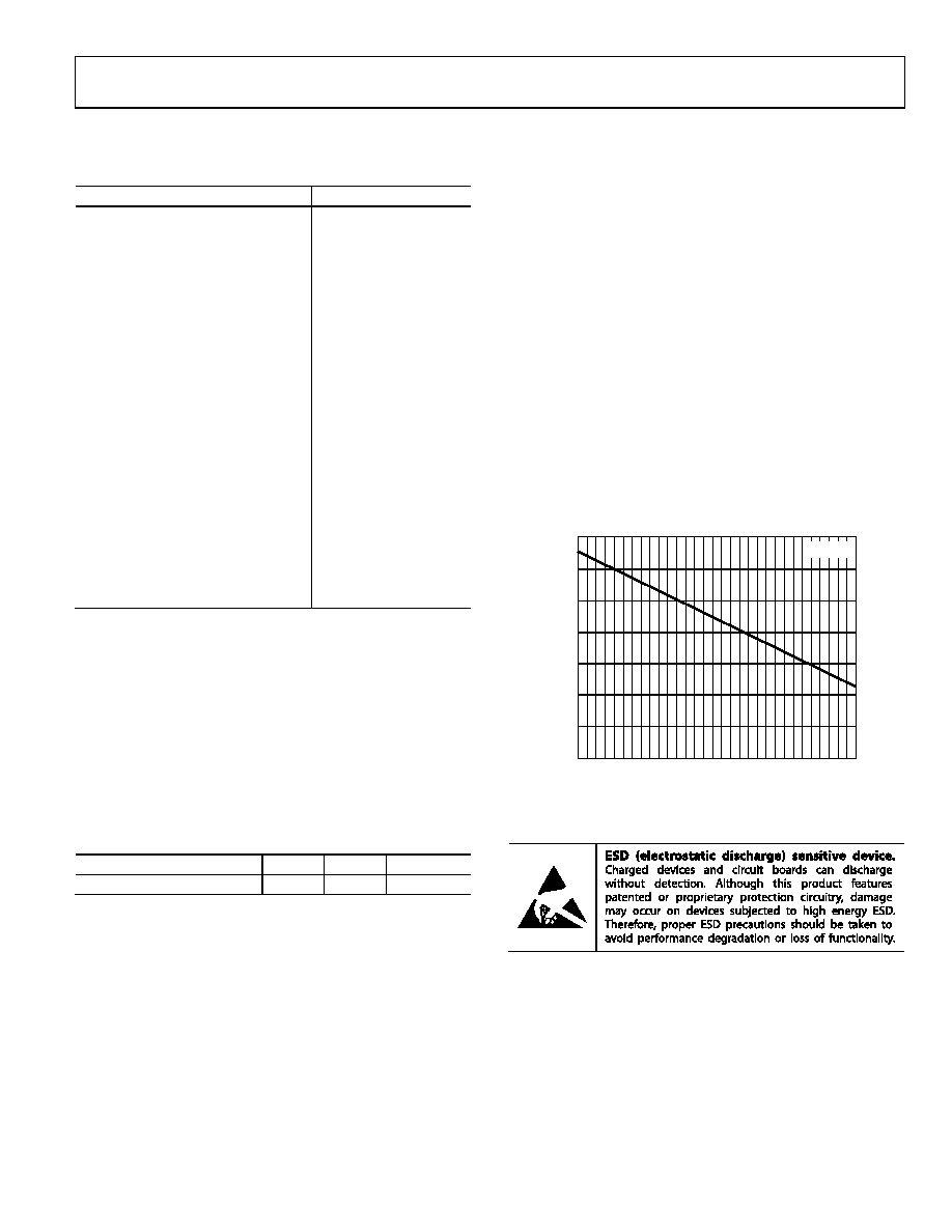
Packaged in the 72-lead LFCSP, the ADV3224/ADV3225 junction-
to-ambient thermal impedance (θJA) is 29°C/W. For long-term
reliability, the maximum allowed junction temperature of the
die should not exceed 125°C; even temporarily exceeding this
limit can cause a shift in parametric performance due to a
change in stresses exerted on the die by the package. Exceeding
a junction temperature of 150°C for an extended period can
result in device failure. In Figure 4, the curve shows the range
of allowed internal die power dissipation that meets these condi-
tions over the 40°C to +85°C ambient temperature range.
When using Figure 4, do not include the external load power
in the maximum power calculation, but do include the load
current dropped on the die output transistors.
0
1
2
3
4
5
6
7
–40
–20
0
20
40
60
80
MA
XI
MU
M
PO
W
ER
D
ISSI
PA
TION
(
W)
AMBIENT TEMPERATURE (°C)
TJ = 150°C
09317-
004
Figure 4. Maximum Die Power Dissipation vs. Ambient Temperature
ESD CAUTION
相关PDF资料 |
PDF描述 |
|---|---|
| ADV3226ACPZ | IC CROSSPOINT SW 16X16 100LFCSP |
| ADV3228ACPZ | IC CROSSPOINT SW 16X8 72LFCSP |
| ADV601LCJSTZ | IC CODEC VIDEO DSP/SRL 120LQFP |
| ADV611JSTZ | IC CCTV DGTL VIDEO CODEC 120LQFP |
| ADV7120KPZ30 | IC DAC VIDEO 3CH 30MHZ 44PLCC |
相关代理商/技术参数 |
参数描述 |
|---|---|
| ADV3226 | 制造商:AD 制造商全称:Analog Devices 功能描述:750 MHz, 16 × 16 Analog Crosspoint Switch |
| ADV3226ACPZ | 功能描述:IC CROSSPOINT SW 16X16 100LFCSP RoHS:是 类别:集成电路 (IC) >> 接口 - 模拟开关,多路复用器,多路分解器 系列:- 其它有关文件:STG4159 View All Specifications 标准包装:5,000 系列:- 功能:开关 电路:1 x SPDT 导通状态电阻:300 毫欧 电压电源:双电源 电压 - 电源,单路/双路(±):±1.65 V ~ 4.8 V 电流 - 电源:50nA 工作温度:-40°C ~ 85°C 安装类型:表面贴装 封装/外壳:7-WFBGA,FCBGA 供应商设备封装:7-覆晶 包装:带卷 (TR) |
| ADV3226-EVALZ | 制造商:AD 制造商全称:Analog Devices 功能描述:750 MHz, 16 × 16 Analog Crosspoint Switch |
| ADV3227 | 制造商:AD 制造商全称:Analog Devices 功能描述:750 MHz, 16 × 16 Analog Crosspoint Switch |
| ADV3227ACPZ | 功能描述:IC CROSSPOINT SW 16X16 100LFCSP RoHS:是 类别:集成电路 (IC) >> 接口 - 模拟开关,多路复用器,多路分解器 系列:- 应用说明:Ultrasound Imaging Systems Application Note 产品培训模块:Lead (SnPb) Finish for COTS Obsolescence Mitigation Program 标准包装:250 系列:- 功能:开关 电路:单刀单掷 导通状态电阻:48 欧姆 电压电源:单电源 电压 - 电源,单路/双路(±):2.7 V ~ 5.5 V 电流 - 电源:5µA 工作温度:0°C ~ 70°C 安装类型:表面贴装 封装/外壳:48-LQFP 供应商设备封装:48-LQFP(7x7) 包装:托盘 |
发布紧急采购,3分钟左右您将得到回复。