- 您现在的位置:买卖IC网 > PDF目录10627 > ADV7180BSTZ (Analog Devices Inc)IC VIDEO DECODER SDTV 64-LQFP PDF资料下载
参数资料
| 型号: | ADV7180BSTZ |
| 厂商: | Analog Devices Inc |
| 文件页数: | 47/116页 |
| 文件大小: | 0K |
| 描述: | IC VIDEO DECODER SDTV 64-LQFP |
| 产品变化通告: | ADV7180 Metal Mask Edit 22/Oct/2009 |
| 设计资源: | Low Cost Differential Video Receiver Using ADA4851 Amplifier and ADV7180 Video Decoder (CN0060) Low Cost Video Multiplexer for Video Switching Using ADA4853-2 Op Amp with Disable Function (CN0076) |
| 标准包装: | 1 |
| 类型: | 视频解码器 |
| 应用: | 数码相机,手机,便携式视频 |
| 安装类型: | 表面贴装 |
| 封装/外壳: | 64-LQFP |
| 供应商设备封装: | 64-LQFP(10x10) |
| 包装: | 托盘 |
| 产品目录页面: | 788 (CN2011-ZH PDF) |
| 配用: | EVAL-ADV7180LQEBZ-ND - BOARD EVALUATION ADV7180 EVAL-ADV7180LFEBZ-ND - BOARD EVAL FOR ADV7180 LFCSP |
第1页第2页第3页第4页第5页第6页第7页第8页第9页第10页第11页第12页第13页第14页第15页第16页第17页第18页第19页第20页第21页第22页第23页第24页第25页第26页第27页第28页第29页第30页第31页第32页第33页第34页第35页第36页第37页第38页第39页第40页第41页第42页第43页第44页第45页第46页当前第47页第48页第49页第50页第51页第52页第53页第54页第55页第56页第57页第58页第59页第60页第61页第62页第63页第64页第65页第66页第67页第68页第69页第70页第71页第72页第73页第74页第75页第76页第77页第78页第79页第80页第81页第82页第83页第84页第85页第86页第87页第88页第89页第90页第91页第92页第93页第94页第95页第96页第97页第98页第99页第100页第101页第102页第103页第104页第105页第106页第107页第108页第109页第110页第111页第112页第113页第114页第115页第116页
ADV7180
Data Sheet
Rev. I | Page 36 of 116
CSFM[2:0], C Shaping Filter Mode, Address 0x17[7:5]
The C shaping filter mode bits allow the user to select from a
range of low-pass filters for the chrominance signal. When
switched in automatic mode, the widest filter is selected based
on the video standard/format and user choice (see Setting 000
and Setting 001 in Table 37).
Table 37. CSFM Function
CSFM[2:0]
Description
000 (default)
Autoselection 1.5 MHz bandwidth
001
Autoselection 2.17 MHz bandwidth
010
SH1
011
SH2
100
SH3
101
SH4
110
SH5
111
Wideband mode
Figure 28 shows the responses of SH1 (narrowest) to SH5
(widest) in addition to the wideband mode (shown in red).
GAIN OPERATION
The gain control within the ADV7180 is done on a purely
digital basis. The input ADC supports a 10-bit range mapped
into a 1.0 V analog voltage range. Gain correction takes place
after the digitization in the form of a digital multiplier.
Advantages of this architecture over the commonly used
programmable gain amplifier (PGA) before the ADC include
the fact that the gain is now completely independent of supply,
temperature, and process variations.
As shown in Figure 30, the ADV7180 can decode a video signal
as long as it fits into the ADC window. The components for this
are the amplitude of the input signal and the dc level it resides on.
The dc level is set by the clamping circuitry (see the Clamp
Operation section).
If the amplitude of the analog video signal is too high, clipping
may occur, resulting in visual artifacts. The analog input range
of the ADC, together with the clamp level, determines the
maximum supported amplitude of the video signal.
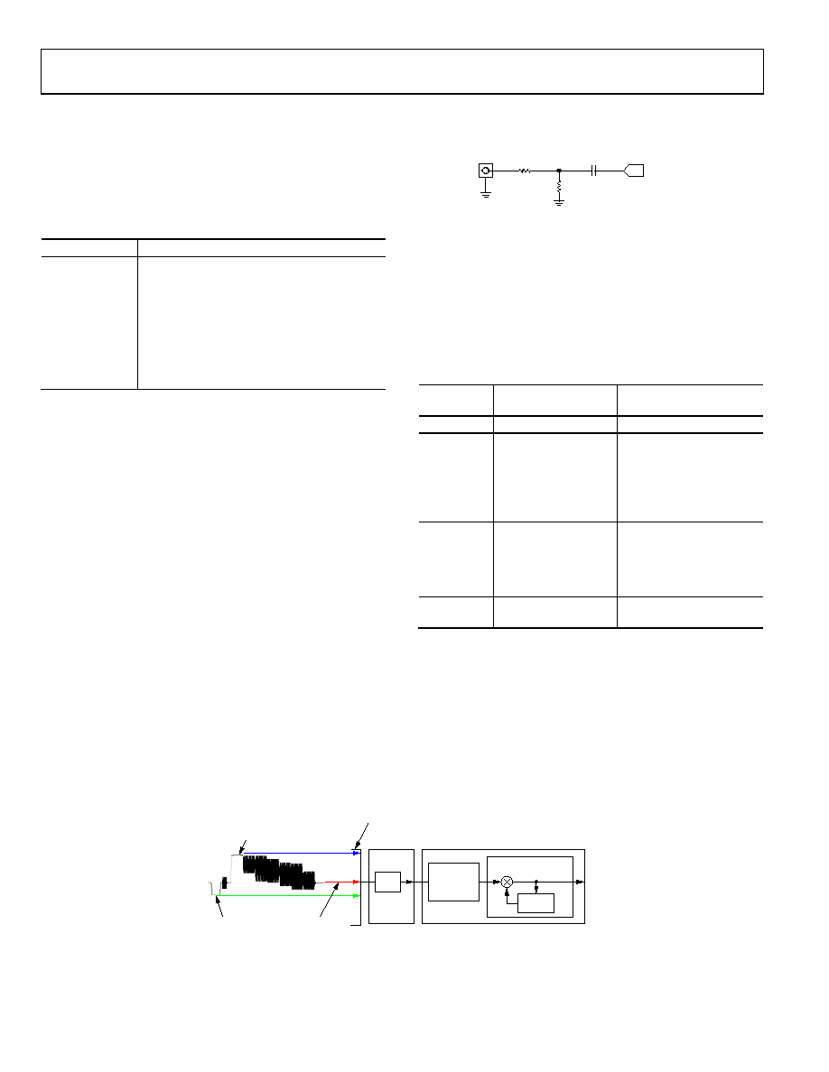
Figure 29 shows a typical voltage divider network that is required
to keep the input video signal within the allowed range of the
ADC, 0 V to 1 V. Place this circuit before all analog inputs to
39
Ω
36
Ω
100nF
ANALOG VIDEO
INPUT
AIN_OF_ADV7180
05700-
024
Figure 29. Input Voltage Divider Network
The minimum supported amplitude of the input video is
determined by the ability of the ADV7180 to retrieve horizontal
and vertical timing and to lock to the color burst, if present.
There are separate gain control units for luma and chroma data.
Both can operate independently of each other. The chroma unit,
however, can also take its gain value from the luma path.
The possible AGC modes are shown in Table 38.
Table 38. AGC Modes
Input
Video Type
Luma Gain
Chroma Gain
Any
Manual gain luma
Manual gain chroma
CVBS
Dependent on
horizontal sync depth
Dependent on color-burst
amplitude taken from
luma path
Peak white
Dependent on color-burst
amplitude taken from
luma path
Y/C
Dependent on
horizontal sync depth
Dependent on color-burst
amplitude taken from
luma path
Peak white
Dependent on color-burst
amplitude
YPrPb
Dependent on
horizontal sync depth
Taken from luma path
It is possible to freeze the automatic gain control loops. This
causes the loops to stop updating and the AGC determined gain
at the time of the freeze to stay active until the loop is either
unfrozen or the gain mode of operation is changed.
The currently active gain from any of the modes can be read
back. Refer to the description of the dual-function manual gain
registers, LG[11:0] luma gain and CG[11:0] chroma gain, in the
Luma Gain and Chroma Gain sections.
ANALOG VOLTAGE
RANGE SUPPORTED BY ADC (1V RANGE FOR ADV7180)
DATA PRE-
PROCESSOR
(DPP)
ADC
VIDEO PROCESSOR
(GAIN SELECTION ONLY)
MAXIMUM
VOLTAGE
MINIMUM
VOLTAGE
CLAMP
LEVEL
GAIN
CONTROL
05700-
025
Figure 30. Gain Control Overview
相关PDF资料 |
PDF描述 |
|---|---|
| VI-BWR-MX-F3 | CONVERTER MOD DC/DC 7.5V 75W |
| VE-2W3-IW-F1 | CONVERTER MOD DC/DC 24V 100W |
| ADV7611BSWZ-P | IC RCVR HDMI 165MHZ LP 64LQFP |
| MAX3483ECPA+ | IC TXRX RS485/422 250KBPS 8-DIP |
| VI-BWR-MX-F1 | CONVERTER MOD DC/DC 7.5V 75W |
相关代理商/技术参数 |
参数描述 |
|---|---|
| ADV7180BSTZ | 制造商:Analog Devices 功能描述:Video IC |
| ADV7180BSTZ-REEL | 功能描述:IC VIDEO DECODER SDTV 64-LQFP RoHS:是 类别:集成电路 (IC) >> 线性 - 视频处理 系列:- 标准包装:250 系列:- 类型:电平移位器 应用:LCD 电视机/监控器 安装类型:表面贴装 封装/外壳:28-WFQFN 裸露焊盘 供应商设备封装:28-WQFN(4x4)裸露焊盘 包装:带卷 (TR) 其它名称:296-32523-2TPS65198RUYT-ND |
| ADV7180KCP32Z | 功能描述:IC VIDEO DECODER 10BIT 32LFCSP RoHS:是 类别:集成电路 (IC) >> 线性 - 视频处理 系列:- 产品变化通告:Product Discontinuation 07/Mar/2011 标准包装:3,000 系列:OMNITUNE™ 类型:调谐器 应用:移动电话,手机,视频显示器 安装类型:表面贴装 封装/外壳:65-WFBGA 供应商设备封装:PG-WFSGA-65 包装:带卷 (TR) 其它名称:SP000365064 |
| ADV7180KCP32Z-RL | 功能描述:IC VIDEO DECODER 10BIT 32LFCSP RoHS:是 类别:集成电路 (IC) >> 线性 - 视频处理 系列:- 产品变化通告:Product Discontinuation 07/Mar/2011 标准包装:3,000 系列:OMNITUNE™ 类型:调谐器 应用:移动电话,手机,视频显示器 安装类型:表面贴装 封装/外壳:65-WFBGA 供应商设备封装:PG-WFSGA-65 包装:带卷 (TR) 其它名称:SP000365064 |
| ADV7180KST48Z | 功能描述:IC VID DECOD SDTV 10BIT 48LQFP RoHS:是 类别:集成电路 (IC) >> 线性 - 视频处理 系列:- 产品变化通告:Product Discontinuation 07/Mar/2011 标准包装:3,000 系列:OMNITUNE™ 类型:调谐器 应用:移动电话,手机,视频显示器 安装类型:表面贴装 封装/外壳:65-WFBGA 供应商设备封装:PG-WFSGA-65 包装:带卷 (TR) 其它名称:SP000365064 |
发布紧急采购,3分钟左右您将得到回复。