- 您现在的位置:买卖IC网 > PDF目录15528 > ADZS-BF537-EZLITE (Analog Devices Inc)BOARD EVAL ADSP-BF537 PDF资料下载
参数资料
| 型号: | ADZS-BF537-EZLITE |
| 厂商: | Analog Devices Inc |
| 文件页数: | 6/68页 |
| 文件大小: | 0K |
| 描述: | BOARD EVAL ADSP-BF537 |
| 产品培训模块: | Interfacing AV Converters to Blackfin Processors Blackfin® Processor Core Architecture Overview Blackfin® Device Drivers Blackfin® Optimizations for Performance and Power Consumption Blackfin® System Services Introduction to VisualDSP++® Tools |
| 特色产品: | Blackfin? BF50x Series Processors |
| 标准包装: | 1 |
| 系列: | Blackfin® |
| 类型: | DSP |
| 适用于相关产品: | ADSP-BF537 |
| 所含物品: | 评估板、软件和说明文档 |
| 配用: | ADZS-BFBLUET-EZEXT-ND - EZ-EXTENDER DAUGHTERBOARD ADZS-BFLLCD-EZEXT-ND - BOARD EXT LANDSCAP LCD INTERFACE ADZS-USBLAN-EZEXT-ND - BOARD DAUGHTER EXTENDED USB-LAN ADZS-BFFPGA-EZEXT-ND - BOARD EVAL FPGA BLACKFIN EXTENDR |
| 相关产品: | ADSP-BF537KBCZ-6BV-ND - IC DSP CTLR 16BIT 208CSPBGA ADSP-BF537BBCZ-5BV-ND - IC DSP CTLR 16BIT 208CSPBGA ADSP-BF537KBCZ-6AV-ND - IC DSP CTLR 16BIT 182CSPBGA ADSP-BF537BBCZ-5AV-ND - IC DSP CTLR 16BIT 182CSPBGA ADSP-BF537BBCZ-5B-ND - IC DSP CTLR 16BIT 208CSPBGA ADSP-BF537BBC-5A-ND - IC DSP CTLR 16BIT 182CSPBGA |
第1页第2页第3页第4页第5页当前第6页第7页第8页第9页第10页第11页第12页第13页第14页第15页第16页第17页第18页第19页第20页第21页第22页第23页第24页第25页第26页第27页第28页第29页第30页第31页第32页第33页第34页第35页第36页第37页第38页第39页第40页第41页第42页第43页第44页第45页第46页第47页第48页第49页第50页第51页第52页第53页第54页第55页第56页第57页第58页第59页第60页第61页第62页第63页第64页第65页第66页第67页第68页
Rev. J
|
Page 14 of 68
|
February 2014
Hibernate State—Maximum Static Power Savings
The hibernate state maximizes static power savings by disabling
the voltage and clocks to the processor core (CCLK) and to all of
the synchronous peripherals (SCLK). The internal voltage regu-
lator for the processor can be shut off by writing b#00 to the
FREQ bits of the VR_CTL register. This disables both CCLK
and SCLK. Furthermore, it sets the internal power supply volt-
age (VDDINT) to 0 V to provide the greatest power savings. To
preserve the processor state, prior to removing power, any criti-
cal information stored internally (memory contents, register
contents, etc.) must be written to a nonvolatile storage device.
Since VDDEXT is still supplied in this state, all of the external pins
three-state, unless otherwise specified. This allows other devices
that are connected to the processor to still have power applied
without drawing unwanted current.
The Ethernet or CAN modules can wake up the internal supply
regulator. If the PH6 pin does not connect as the PHYINT sig-
nal to an external PHY device, it can be pulled low by any other
device to wake the processor up. The regulator can also be
woken up by a real-time clock wake-up event or by asserting the
RESET pin. All hibernate wake-up events initiate the hardware
reset sequence. Individual sources are enabled by the VR_CTL
register.
With the exception of the VR_CTL and the RTC registers, all
internal registers and memories lose their content in the hiber-
nate state. State variables can be held in external SRAM or
SDRAM. The SCKELOW bit in the VR_CTL register provides a
means of waking from hibernate state without disrupting a self-
refreshing SDRAM, provided that there is also an external pull-
down on the SCKE pin.
Power Savings
As shown in Table 5, the processors support three different
power domains which maximizes flexibility, while maintaining
compliance with industry standards and conventions. By isolat-
ing the internal logic of the processor into its own power
domain, separate from the RTC and other I/O, the processor
can take advantage of dynamic power management, without
affecting the RTC or other I/O devices. There are no sequencing
requirements for the various power domains.
The dynamic power management feature allows both the pro-
cessor’s input voltage (VDDINT) and clock frequency (fCCLK) to be
dynamically controlled.
The power dissipated by a processor is largely a function of its
clock frequency and the square of the operating voltage. For
example, reducing the clock frequency by 25% results in a 25%
reduction in power dissipation, while reducing the voltage by
25% reduces power dissipation by more than 40%. Further,
these power savings are additive, in that if the clock frequency
and supply voltage are both reduced, the power savings can be
dramatic, as shown in the following equations.
The power savings factor (PSF) is calculated as:
where:
fCCLKNOM is the nominal core clock frequency
fCCLKRED is the reduced core clock frequency
VDDINTNOM is the nominal internal supply voltage
VDDINTRED is the reduced internal supply voltage
tNOM is the duration running at fCCLKNOM
tRED is the duration running at fCCLKRED
The percent power savings is calculated as
VOLTAGE REGULATION
The ADSP-BF534/ADSP-BF536/ADSP-BF537 processors pro-
vide an on-chip voltage regulator that can generate appropriate
Conditions on Page 23 for regulator tolerances and acceptable
VDDEXT ranges for specific models.
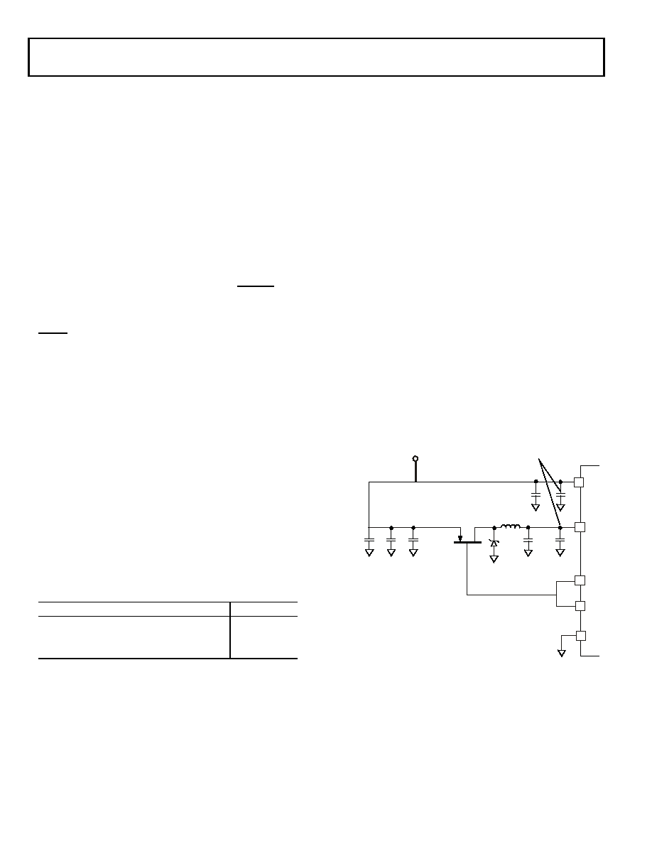
Figure 5 shows the typical external components required to
complete the power management system. The regulator con-
trols the internal logic voltage levels and is programmable with
the voltage regulator control register (VR_CTL) in increments
of 50 mV. To reduce standby power consumption, the internal
voltage regulator can be programmed to remove power to the
processor core while keeping I/O power supplied. While in
Table 5. Power Domains
Power Domain
VDD Range
All internal logic, except RTC
VDDINT
RTC internal logic and crystal I/O
VDDRTC
All other I/O
VDDEXT
Figure 5. Voltage Regulator Circuit
PSF
fCCLKRED
fCCLKNOM
---------------------
VDDINTRED
VDDINTNOM
--------------------------
2
tRED
tNOM
-----------
=
% power savings
1
PSF
–
100%
=
VDDEXT
(LOW-INDUCTANCE)
VDDINT
VROUT
100μF
VROUT
GND
SHORT AND LOW-
INDUCTANCE WIRE
VDDEXT
+
100μF
10μF
LOW ESR
100nF
SET OF DECOUPLING
CAPACITORS
FDS9431A
ZHCS1000
NOTE: DESIGNER SHOULD MINIMIZE
TRACE LENGTH TO FDS9431A.
10μH
相关PDF资料 |
PDF描述 |
|---|---|
| ECM15DSEI-S243 | CONN EDGECARD 30POS .156 EYELET |
| ADZS-BF518F-EZBRD | BOARD EVAL BF512F/14F/16F/18F |
| ADZS-BF526-EZBRD | BOARD EVAL NO DEBUG BF526 |
| GCM18DTBN-S189 | CONN EDGECARD 36POS R/A .156 SLD |
| GCM18DTBH-S189 | CONN EDGECARD 36POS R/A .156 SLD |
相关代理商/技术参数 |
参数描述 |
|---|---|
| ADZS-BF537-STAMP | 功能描述:SYSTEM DEV FOR ADSP-BF537 RoHS:是 类别:编程器,开发系统 >> 通用嵌入式开发板和套件(MCU、DSP、FPGA、CPLD等) 系列:Blackfin® 产品培训模块:Blackfin® Processor Core Architecture Overview Blackfin® Device Drivers Blackfin® Optimizations for Performance and Power Consumption Blackfin® System Services 特色产品:Blackfin? BF50x Series Processors 标准包装:1 系列:Blackfin® 类型:DSP 适用于相关产品:ADSP-BF548 所含物品:板,软件,4x4 键盘,光学拨轮,QVGA 触摸屏 LCD 和 40G 硬盘 配用:ADZS-BFBLUET-EZEXT-ND - EZ-EXTENDER DAUGHTERBOARDADZS-BFLLCD-EZEXT-ND - BOARD EXT LANDSCAP LCD INTERFACE 相关产品:ADSP-BF542BBCZ-4A-ND - IC DSP 16BIT 400MHZ 400CSBGAADSP-BF544MBBCZ-5M-ND - IC DSP 16BIT 533MHZ MDDR 400CBGAADSP-BF542MBBCZ-5M-ND - IC DSP 16BIT 533MHZ MDDR 400CBGAADSP-BF542KBCZ-6A-ND - IC DSP 16BIT 600MHZ 400CSBGAADSP-BF547MBBCZ-5M-ND - IC DSP 16BIT 533MHZ MDDR 400CBGAADSP-BF548BBCZ-5A-ND - IC DSP 16BIT 533MHZ 400CSBGAADSP-BF547BBCZ-5A-ND - IC DSP 16BIT 533MHZ 400CSBGAADSP-BF544BBCZ-5A-ND - IC DSP 16BIT 533MHZ 400CSBGAADSP-BF542BBCZ-5A-ND - IC DSP 16BIT 533MHZ 400CSBGA |
| ADZS-BF537-STAMP | 制造商:Analog Devices 功能描述:Microcontroller Development Tool |
| ADZS-BF538-EZLITE | 制造商:Analog Devices 功能描述:- Bulk |
| ADZSBF538FEZLITE | 制造商:Analog Devices 功能描述:RES Wirewound 6927 75Ohm 1% 3W 20PPM SMD T/R |
| ADZS-BF538F-EZLITE | 功能描述:BOARD EVAL FOR ADSP-BF538 RoHS:否 类别:编程器,开发系统 >> 通用嵌入式开发板和套件(MCU、DSP、FPGA、CPLD等) 系列:Blackfin® 产品培训模块:Blackfin® Processor Core Architecture Overview Blackfin® Device Drivers Blackfin® Optimizations for Performance and Power Consumption Blackfin® System Services 特色产品:Blackfin? BF50x Series Processors 标准包装:1 系列:Blackfin® 类型:DSP 适用于相关产品:ADSP-BF548 所含物品:板,软件,4x4 键盘,光学拨轮,QVGA 触摸屏 LCD 和 40G 硬盘 配用:ADZS-BFBLUET-EZEXT-ND - EZ-EXTENDER DAUGHTERBOARDADZS-BFLLCD-EZEXT-ND - BOARD EXT LANDSCAP LCD INTERFACE 相关产品:ADSP-BF542BBCZ-4A-ND - IC DSP 16BIT 400MHZ 400CSBGAADSP-BF544MBBCZ-5M-ND - IC DSP 16BIT 533MHZ MDDR 400CBGAADSP-BF542MBBCZ-5M-ND - IC DSP 16BIT 533MHZ MDDR 400CBGAADSP-BF542KBCZ-6A-ND - IC DSP 16BIT 600MHZ 400CSBGAADSP-BF547MBBCZ-5M-ND - IC DSP 16BIT 533MHZ MDDR 400CBGAADSP-BF548BBCZ-5A-ND - IC DSP 16BIT 533MHZ 400CSBGAADSP-BF547BBCZ-5A-ND - IC DSP 16BIT 533MHZ 400CSBGAADSP-BF544BBCZ-5A-ND - IC DSP 16BIT 533MHZ 400CSBGAADSP-BF542BBCZ-5A-ND - IC DSP 16BIT 533MHZ 400CSBGA |
发布紧急采购,3分钟左右您将得到回复。