- 您现在的位置:买卖IC网 > PDF目录15528 > ADZS-BF537-EZLITE (Analog Devices Inc)BOARD EVAL ADSP-BF537 PDF资料下载
参数资料
| 型号: | ADZS-BF537-EZLITE |
| 厂商: | Analog Devices Inc |
| 文件页数: | 7/68页 |
| 文件大小: | 0K |
| 描述: | BOARD EVAL ADSP-BF537 |
| 产品培训模块: | Interfacing AV Converters to Blackfin Processors Blackfin® Processor Core Architecture Overview Blackfin® Device Drivers Blackfin® Optimizations for Performance and Power Consumption Blackfin® System Services Introduction to VisualDSP++® Tools |
| 特色产品: | Blackfin? BF50x Series Processors |
| 标准包装: | 1 |
| 系列: | Blackfin® |
| 类型: | DSP |
| 适用于相关产品: | ADSP-BF537 |
| 所含物品: | 评估板、软件和说明文档 |
| 配用: | ADZS-BFBLUET-EZEXT-ND - EZ-EXTENDER DAUGHTERBOARD ADZS-BFLLCD-EZEXT-ND - BOARD EXT LANDSCAP LCD INTERFACE ADZS-USBLAN-EZEXT-ND - BOARD DAUGHTER EXTENDED USB-LAN ADZS-BFFPGA-EZEXT-ND - BOARD EVAL FPGA BLACKFIN EXTENDR |
| 相关产品: | ADSP-BF537KBCZ-6BV-ND - IC DSP CTLR 16BIT 208CSPBGA ADSP-BF537BBCZ-5BV-ND - IC DSP CTLR 16BIT 208CSPBGA ADSP-BF537KBCZ-6AV-ND - IC DSP CTLR 16BIT 182CSPBGA ADSP-BF537BBCZ-5AV-ND - IC DSP CTLR 16BIT 182CSPBGA ADSP-BF537BBCZ-5B-ND - IC DSP CTLR 16BIT 208CSPBGA ADSP-BF537BBC-5A-ND - IC DSP CTLR 16BIT 182CSPBGA |
第1页第2页第3页第4页第5页第6页当前第7页第8页第9页第10页第11页第12页第13页第14页第15页第16页第17页第18页第19页第20页第21页第22页第23页第24页第25页第26页第27页第28页第29页第30页第31页第32页第33页第34页第35页第36页第37页第38页第39页第40页第41页第42页第43页第44页第45页第46页第47页第48页第49页第50页第51页第52页第53页第54页第55页第56页第57页第58页第59页第60页第61页第62页第63页第64页第65页第66页第67页第68页
Rev. J
|
Page 15 of 68
|
February 2014
hibernate state, VDDEXT can still be applied, eliminating the need
for external buffers. The voltage regulator can be activated from
this power-down state by asserting the RESET pin, which then
initiates a boot sequence. The regulator can also be disabled and
bypassed at the user’s discretion. For additional information on
voltage regulation, see Switching Regulator Design Consider-
ations for the ADSP-BF533 Blackfin Processors (EE-228).
CLOCK SIGNALS
The ADSP-BF534/ADSP-BF536/ADSP-BF537 processors can
be clocked by an external crystal, a sine wave input, or a buff-
ered, shaped clock derived from an external clock oscillator.
If an external clock is used, it should be a TTL compatible signal
and must not be halted, changed, or operated below the speci-
fied frequency during normal operation. This signal is
connected to the processor’s CLKIN pin. When an external
clock is used, the XTAL pin must be left unconnected.
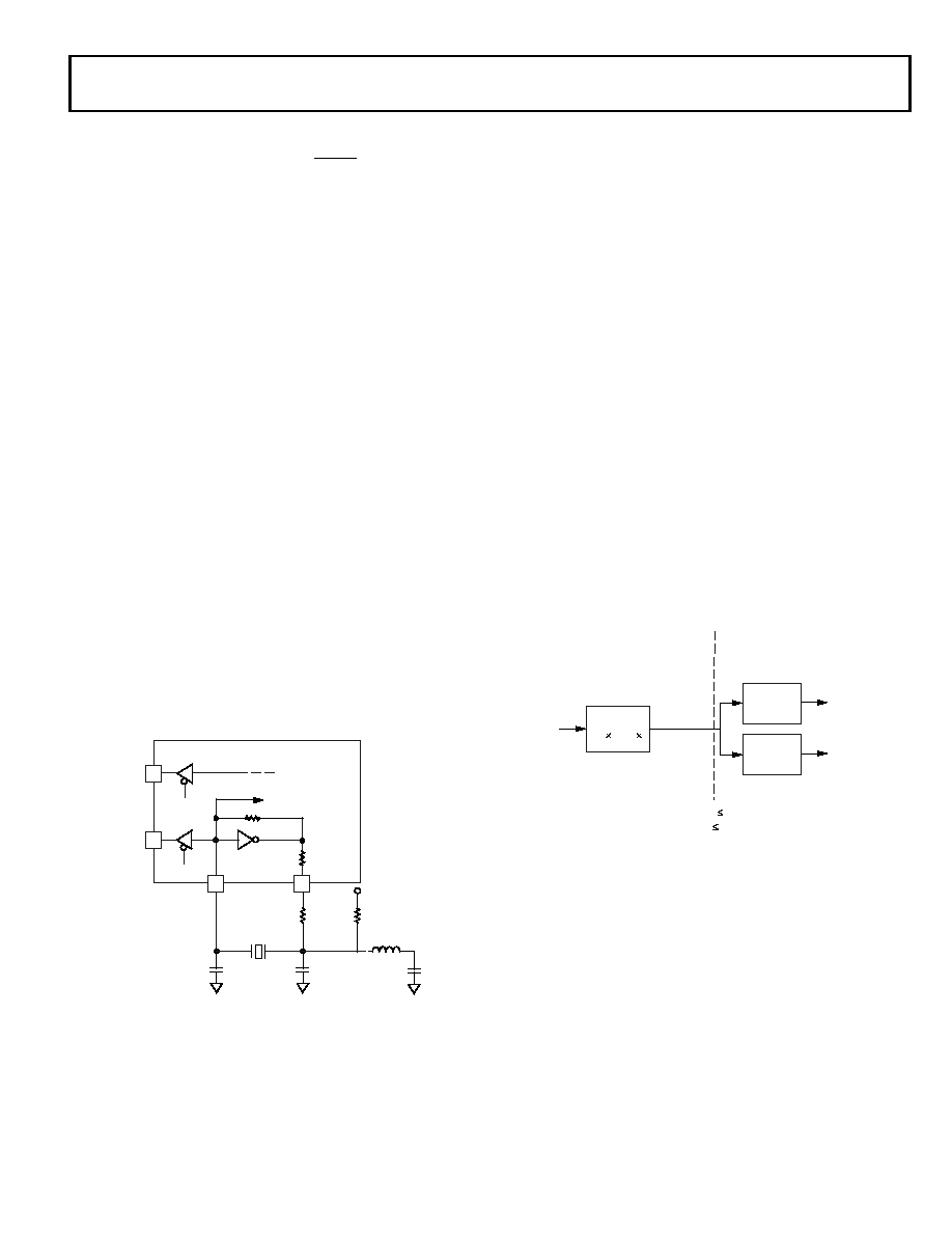
Alternatively, because the processors include an on-chip oscilla-
tor circuit, an external crystal can be used. For fundamental
frequency operation, use the circuit shown in Figure 6. A
parallel-resonant, fundamental frequency, microprocessor-
grade crystal is connected across the CLKIN and XTAL pins.
The on-chip resistance between CLKIN and the XTAL pin is in
the 500 k range. Further parallel resistors are typically not rec-
ommended. The two capacitors and the series resistor shown in
Figure 6 fine-tune phase and amplitude of the sine frequency.
The capacitor and resistor values shown in Figure 6 are typical
values only. The capacitor values are dependent upon the crystal
manufacturers’ load capacitance recommendations and the PCB
physical layout. The resistor value depends on the drive level
specified by the crystal manufacturer. The user should verify the
customized values based on careful investigations of multiple
devices over temperature range.
A third-overtone crystal can be used for frequencies above
25 MHz. The circuit is then modified to ensure crystal operation
only at the third overtone, by adding a tuned inductor circuit as
shown in Figure 6. A design procedure for third-overtone oper-
ation is discussed in detail in the application note Using Third
Overtone Crystals with the ADSP-218x DSP (EE-168).
The CLKBUF pin is an output pin, and is a buffer version of the
input clock. This pin is particularly useful in Ethernet applica-
tions to limit the number of required clock sources in the
system. In this type of application, a single 25 MHz or 50 MHz
crystal can be applied directly to the processors. The 25 MHz or
50 MHz output of CLKBUF can then be connected to an exter-
nal Ethernet MII or RMII PHY device.
Because of the default 10× PLL multiplier, providing a 50 MHz
CLKIN exceeds the recommended operating conditions of the
lower speed grades. Because of this restriction, an RMII PHY
requiring a 50 MHz clock input cannot be clocked directly from
the CLKBUF pin for the lower speed grades. In this case, either
provide a separate 50 MHz clock source, or use an RMII PHY
with 25 MHz clock input options. The CLKBUF output is active
by default and can be disabled using the VR_CTL register for
power savings.
The Blackfin core runs at a different clock rate than the on-chip
peripherals. As shown in Figure 7, the core clock (CCLK) and
system peripheral clock (SCLK) are derived from the input
clock (CLKIN) signal. An on-chip PLL is capable of multiplying
the CLKIN signal by a programmable 0.5× to 64× multiplication
factor (bounded by specified minimum and maximum VCO
frequencies). The default multiplier is 10×, but it can be modi-
fied by a software instruction sequence in the PLL_CTL register.
On-the-fly CCLK and SCLK frequency changes can be effected
by simply writing to the PLL_DIV register. Whereas the maxi-
mum allowed CCLK and SCLK rates depend on the applied
voltages VDDINT and VDDEXT, the VCO is always permitted to run
up to the frequency specified by the part’s speed grade. The
CLKOUT pin reflects the SCLK frequency to the off-chip world.
It belongs to the SDRAM interface, but it functions as a refer-
ence signal in other timing specifications as well. While active
by default, it can be disabled using the EBIU_SDGCTL and
EBIU_AMGCTL registers.
All on-chip peripherals are clocked by the system clock (SCLK).
The system clock frequency is programmable by means of the
SSEL3–0 bits of the PLL_DIV register. The values programmed
into the SSEL fields define a divide ratio between the PLL output
Figure 6. External Crystal Connections
CLKIN
CLKOUT
XTAL
EN
CLKBUF
TO PLL CIRCUITRY
FOR OVERTONE
OPERATION ONLY:
NOTE: VALUES MARKED WITH * MUST BE CUSTOMIZED, DEPENDING
ON THE CRYSTAL AND LAYOUT. PLEASE ANALYZE CAREFULLY.
18 pF *
EN
18 pF *
330
*
BLACKFIN
350
1M
V
DDEXT
Figure 7. Frequency Modification Methods
PLL
0.5 to 64
÷1 to 15
÷1,2, 4, 8
VCO
CLKIN
“FINE” ADJUSTMENT
REQUIRES PLL SEQUENCING
“COARSE” ADJUSTMENT
ON-THE-FLY
CCLK
SCLK
CCLK
SCLK
133 MHz
相关PDF资料 |
PDF描述 |
|---|---|
| ECM15DSEI-S243 | CONN EDGECARD 30POS .156 EYELET |
| ADZS-BF518F-EZBRD | BOARD EVAL BF512F/14F/16F/18F |
| ADZS-BF526-EZBRD | BOARD EVAL NO DEBUG BF526 |
| GCM18DTBN-S189 | CONN EDGECARD 36POS R/A .156 SLD |
| GCM18DTBH-S189 | CONN EDGECARD 36POS R/A .156 SLD |
相关代理商/技术参数 |
参数描述 |
|---|---|
| ADZS-BF537-STAMP | 功能描述:SYSTEM DEV FOR ADSP-BF537 RoHS:是 类别:编程器,开发系统 >> 通用嵌入式开发板和套件(MCU、DSP、FPGA、CPLD等) 系列:Blackfin® 产品培训模块:Blackfin® Processor Core Architecture Overview Blackfin® Device Drivers Blackfin® Optimizations for Performance and Power Consumption Blackfin® System Services 特色产品:Blackfin? BF50x Series Processors 标准包装:1 系列:Blackfin® 类型:DSP 适用于相关产品:ADSP-BF548 所含物品:板,软件,4x4 键盘,光学拨轮,QVGA 触摸屏 LCD 和 40G 硬盘 配用:ADZS-BFBLUET-EZEXT-ND - EZ-EXTENDER DAUGHTERBOARDADZS-BFLLCD-EZEXT-ND - BOARD EXT LANDSCAP LCD INTERFACE 相关产品:ADSP-BF542BBCZ-4A-ND - IC DSP 16BIT 400MHZ 400CSBGAADSP-BF544MBBCZ-5M-ND - IC DSP 16BIT 533MHZ MDDR 400CBGAADSP-BF542MBBCZ-5M-ND - IC DSP 16BIT 533MHZ MDDR 400CBGAADSP-BF542KBCZ-6A-ND - IC DSP 16BIT 600MHZ 400CSBGAADSP-BF547MBBCZ-5M-ND - IC DSP 16BIT 533MHZ MDDR 400CBGAADSP-BF548BBCZ-5A-ND - IC DSP 16BIT 533MHZ 400CSBGAADSP-BF547BBCZ-5A-ND - IC DSP 16BIT 533MHZ 400CSBGAADSP-BF544BBCZ-5A-ND - IC DSP 16BIT 533MHZ 400CSBGAADSP-BF542BBCZ-5A-ND - IC DSP 16BIT 533MHZ 400CSBGA |
| ADZS-BF537-STAMP | 制造商:Analog Devices 功能描述:Microcontroller Development Tool |
| ADZS-BF538-EZLITE | 制造商:Analog Devices 功能描述:- Bulk |
| ADZSBF538FEZLITE | 制造商:Analog Devices 功能描述:RES Wirewound 6927 75Ohm 1% 3W 20PPM SMD T/R |
| ADZS-BF538F-EZLITE | 功能描述:BOARD EVAL FOR ADSP-BF538 RoHS:否 类别:编程器,开发系统 >> 通用嵌入式开发板和套件(MCU、DSP、FPGA、CPLD等) 系列:Blackfin® 产品培训模块:Blackfin® Processor Core Architecture Overview Blackfin® Device Drivers Blackfin® Optimizations for Performance and Power Consumption Blackfin® System Services 特色产品:Blackfin? BF50x Series Processors 标准包装:1 系列:Blackfin® 类型:DSP 适用于相关产品:ADSP-BF548 所含物品:板,软件,4x4 键盘,光学拨轮,QVGA 触摸屏 LCD 和 40G 硬盘 配用:ADZS-BFBLUET-EZEXT-ND - EZ-EXTENDER DAUGHTERBOARDADZS-BFLLCD-EZEXT-ND - BOARD EXT LANDSCAP LCD INTERFACE 相关产品:ADSP-BF542BBCZ-4A-ND - IC DSP 16BIT 400MHZ 400CSBGAADSP-BF544MBBCZ-5M-ND - IC DSP 16BIT 533MHZ MDDR 400CBGAADSP-BF542MBBCZ-5M-ND - IC DSP 16BIT 533MHZ MDDR 400CBGAADSP-BF542KBCZ-6A-ND - IC DSP 16BIT 600MHZ 400CSBGAADSP-BF547MBBCZ-5M-ND - IC DSP 16BIT 533MHZ MDDR 400CBGAADSP-BF548BBCZ-5A-ND - IC DSP 16BIT 533MHZ 400CSBGAADSP-BF547BBCZ-5A-ND - IC DSP 16BIT 533MHZ 400CSBGAADSP-BF544BBCZ-5A-ND - IC DSP 16BIT 533MHZ 400CSBGAADSP-BF542BBCZ-5A-ND - IC DSP 16BIT 533MHZ 400CSBGA |
发布紧急采购,3分钟左右您将得到回复。