- 您现在的位置:买卖IC网 > PDF目录235794 > AGLE600V5-FG256C FPGA, 13824 CLBS, 600000 GATES, PBGA256 PDF资料下载
参数资料
| 型号: | AGLE600V5-FG256C |
| 元件分类: | FPGA |
| 英文描述: | FPGA, 13824 CLBS, 600000 GATES, PBGA256 |
| 封装: | 17 X 17 MM, 1.60 MM HEIGHT, 1 MM PITCH, FBGA-256 |
| 文件页数: | 87/156页 |
| 文件大小: | 5023K |
| 代理商: | AGLE600V5-FG256C |
第1页第2页第3页第4页第5页第6页第7页第8页第9页第10页第11页第12页第13页第14页第15页第16页第17页第18页第19页第20页第21页第22页第23页第24页第25页第26页第27页第28页第29页第30页第31页第32页第33页第34页第35页第36页第37页第38页第39页第40页第41页第42页第43页第44页第45页第46页第47页第48页第49页第50页第51页第52页第53页第54页第55页第56页第57页第58页第59页第60页第61页第62页第63页第64页第65页第66页第67页第68页第69页第70页第71页第72页第73页第74页第75页第76页第77页第78页第79页第80页第81页第82页第83页第84页第85页第86页当前第87页第88页第89页第90页第91页第92页第93页第94页第95页第96页第97页第98页第99页第100页第101页第102页第103页第104页第105页第106页第107页第108页第109页第110页第111页第112页第113页第114页第115页第116页第117页第118页第119页第120页第121页第122页第123页第124页第125页第126页第127页第128页第129页第130页第131页第132页第133页第134页第135页第136页第137页第138页第139页第140页第141页第142页第143页第144页第145页第146页第147页第148页第149页第150页第151页第152页第153页第154页第155页第156页
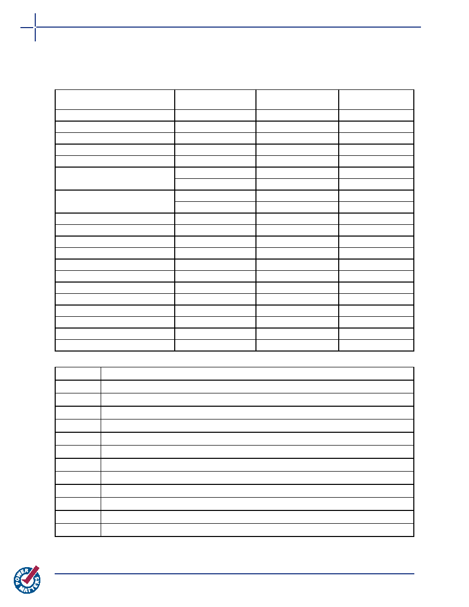
IGLOOe DC and Switching Characteristics
2- 22
Advance v0.3
Summary of I/O Timing Characteristics – Default I/O Software
Settings
Table 2-22 Summary of AC Measuring Points
Standard
Input Reference
Voltage (VREF_TYP)
Board Termination
Voltage (VTT_REF)
Measuring Trip
Point (Vtrip)
3.3 V LVTTL / 3.3 V LVCMOS
–
1.4 V
2.5 V LVCMOS
–
1.2 V
1.8 V LVCMOS
–
0.90 V
1.5 V LVCMOS
–
0.75 V
1.2 V LVCMOS
–
0.6 V
3.3 V PCI
–
0.285*VCCI (RR)
–
0.615*VCCI (FF))
3.3 V PCI-X
–
0.285*VCCI (RR)
–
0.615*VCCI (FF)
3.3 V GTL
0.8 V
1.2 V
VREF
2.5 V GTL
0.8 V
1.2 V
VREF
3.3 V GTL+
1.0 V
1.5 V
VREF
2.5 V GTL+
1.0 V
1.5 V
VREF
HSTL (I)
0.75 V
VREF
HSTL (II)
0.75 V
VREF
SSTL2 (I)
1.25 V
VREF
SSTL2 (II)
1.25 V
VREF
SSTL3 (I)
1.5 V
1.485 V
VREF
SSTL3 (II)
1.5 V
1.485 V
VREF
LVDS
–
Cross point
LVPECL
–
Cross point
Table 2-23 I/O AC Parameter Definitions
Parameter
Definition
tDP
Data to Pad delay through the Output Buffer
tPY
Pad to Data delay through the Input Buffer with Schmitt trigger disabled
tDOUT
Data to Output Buffer delay through the I/O interface
tEOUT
Enable to Output Buffer Tristate Control delay through the I/O interface
tDIN
Input Buffer to Data delay through the I/O interface
tPYS
Pad to Data delay through the Input Buffer with Schmitt trigger enabled
tHZ
Enable to Pad delay through the Output Buffer—HIGH to Z
tZH
Enable to Pad delay through the Output Buffer—Z to HIGH
tLZ
Enable to Pad delay through the Output Buffer—LOW to Z
tZL
Enable to Pad delay through the Output Buffer—Z to LOW
tZHS
Enable to Pad delay through the Output Buffer with delayed enable—Z to HIGH
tZLS
Enable to Pad delay through the Output Buffer with delayed enable—Z to LOW
相关PDF资料 |
PDF描述 |
|---|---|
| AGLE600V5-FG484C | FPGA, 13824 CLBS, 600000 GATES, PBGA484 |
| AGLE600V5-FGG256C | FPGA, 13824 CLBS, 600000 GATES, PBGA256 |
| AGLE600V5-FGG484C | FPGA, 13824 CLBS, 600000 GATES, PBGA484 |
| ACBQ20TTEB270K/390M | RC NETWORK, BUSSED, 1W, 27ohm, 20V, 0.000039uF, SURFACE MOUNT, 20 |
| ACBQ20TTEB270K/401M | RC NETWORK, BUSSED, 1W, 27ohm, 20V, 0.0004uF, SURFACE MOUNT, 20 |
相关代理商/技术参数 |
参数描述 |
|---|---|
| AGLE600V5-FG256I | 功能描述:IC FPGA 1KB FLASH 600K 256-FBGA RoHS:否 类别:集成电路 (IC) >> 嵌入式 - FPGA(现场可编程门阵列) 系列:IGLOOe 产品培训模块:Three Reasons to Use FPGA's in Industrial Designs Cyclone IV FPGA Family Overview 特色产品:Cyclone? IV FPGAs 标准包装:60 系列:CYCLONE® IV GX LAB/CLB数:9360 逻辑元件/单元数:149760 RAM 位总计:6635520 输入/输出数:270 门数:- 电源电压:1.16 V ~ 1.24 V 安装类型:表面贴装 工作温度:0°C ~ 85°C 封装/外壳:484-BGA 供应商设备封装:484-FBGA(23x23) |
| AGLE600V5-FG484 | 功能描述:IC FPGA 1KB FLASH 600K 484-FBGA RoHS:否 类别:集成电路 (IC) >> 嵌入式 - FPGA(现场可编程门阵列) 系列:IGLOOe 标准包装:40 系列:SX-A LAB/CLB数:6036 逻辑元件/单元数:- RAM 位总计:- 输入/输出数:360 门数:108000 电源电压:2.25 V ~ 5.25 V 安装类型:表面贴装 工作温度:0°C ~ 70°C 封装/外壳:484-BGA 供应商设备封装:484-FPBGA(27X27) |
| AGLE600V5-FG484I | 功能描述:IC FPGA 1KB FLASH 600K 484-FBGA RoHS:否 类别:集成电路 (IC) >> 嵌入式 - FPGA(现场可编程门阵列) 系列:IGLOOe 产品培训模块:Three Reasons to Use FPGA's in Industrial Designs Cyclone IV FPGA Family Overview 特色产品:Cyclone? IV FPGAs 标准包装:60 系列:CYCLONE® IV GX LAB/CLB数:9360 逻辑元件/单元数:149760 RAM 位总计:6635520 输入/输出数:270 门数:- 电源电压:1.16 V ~ 1.24 V 安装类型:表面贴装 工作温度:0°C ~ 85°C 封装/外壳:484-BGA 供应商设备封装:484-FBGA(23x23) |
| AGLE600V5-FG896 | 制造商:ACTEL 制造商全称:Actel Corporation 功能描述:IGLOOe Low-Power Flash FPGAs with Flash Freeze Technology |
| AGLE600V5-FG896ES | 制造商:ACTEL 制造商全称:Actel Corporation 功能描述:IGLOOe Low-Power Flash FPGAs with Flash Freeze Technology |
发布紧急采购,3分钟左右您将得到回复。