- 您现在的位置:买卖IC网 > PDF目录64108 > AH114-89G 60 MHz - 2500 MHz RF/MICROWAVE WIDE BAND MEDIUM POWER AMPLIFIER PDF资料下载
参数资料
| 型号: | AH114-89G |
| 元件分类: | 放大器 |
| 英文描述: | 60 MHz - 2500 MHz RF/MICROWAVE WIDE BAND MEDIUM POWER AMPLIFIER |
| 封装: | GREEN, TO-243C, SOT-89, SMT, 3 PIN |
| 文件页数: | 2/6页 |
| 文件大小: | 199K |
| 代理商: | AH114-89G |
Specifications and information are subject to change without notice
WJ Communications, Inc
Phone 1-800-WJ1-4401 FAX: 408-577-6621 e-mail: sales@wj.com Web site: www.wj.com, www.TriQuint.com
Page 2 of 6 January 2008
AH114
Watt, High Linearity InGaP HBT Amplifier
Typical Device Data
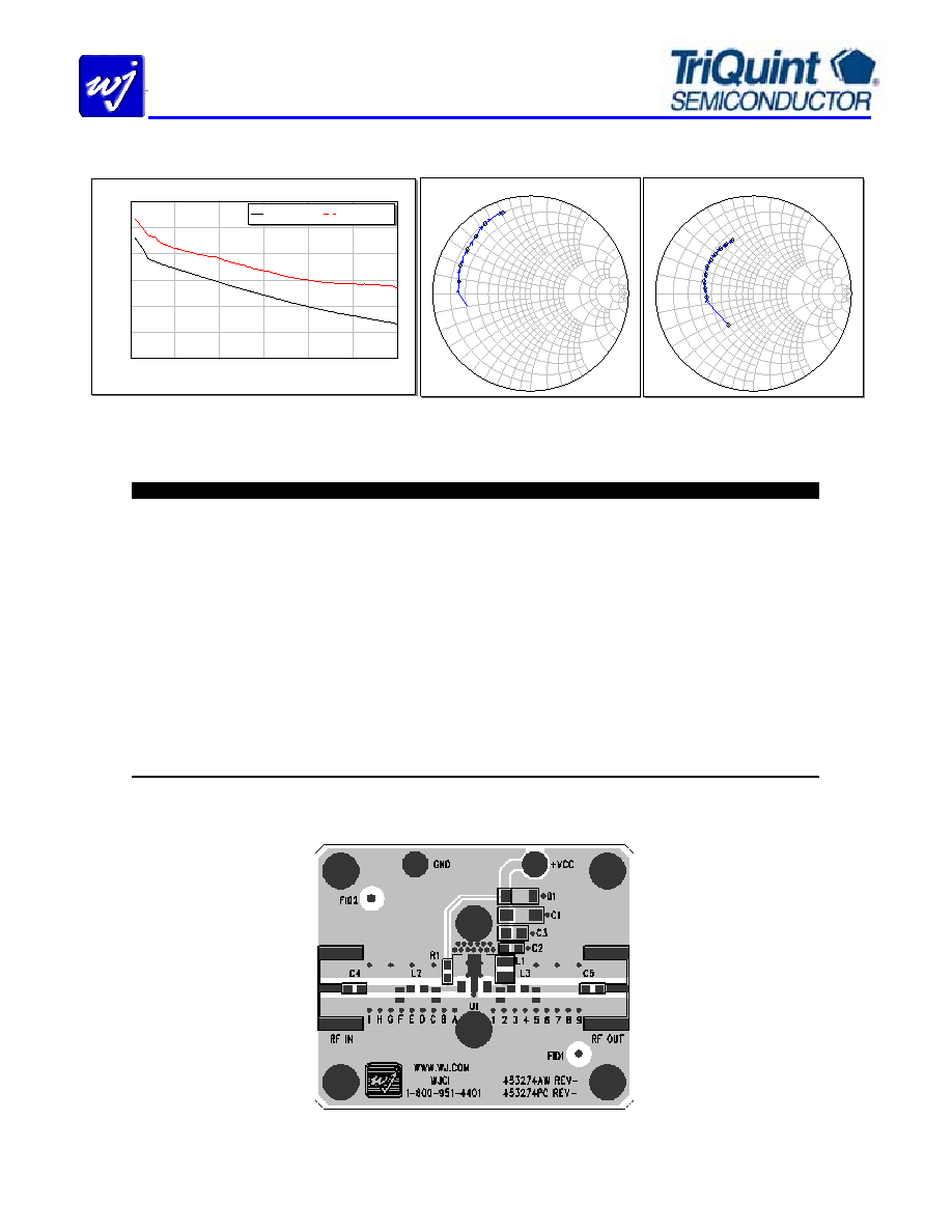
S-Parameters (Vcc = +5 V, Icc = 150 mA, T = 25
°C, unmatched 50 ohm system)
0
0.5
1
1.5
2
2.5
3
Frequency (GHz)
Gain / Maximum Stable Gain
0
5
10
15
20
25
30
Ga
in
(d
B
)
DB(|S[2,1]|) *
DB(GMax) *
0
1.
0
1.
0
-1
.
0
10
.
0
10.0
-1
0.
0
5.
0
5.
0
-5
.0
2.
0
2
.
0
-
2
.
0
3.
0
3.
0
-3
.
0
4.
0
4.
0
-4
.0
0.
2
0.
2
-0
.2
0.
4
0
.4
-
0.
4
0.
6
0
.
6
-
0
.
6
0.
8
0
.
8
-
0
.
8
S11
Swp Max
3.075GHz
Swp Min
0.05GHz
0
1.
0
1.
0
-1
.
0
10
.
0
10.0
-1
0.
0
5.
0
5.
0
-5
.0
2.
0
2
.
0
-
2
.
0
3.
0
3.
0
-3
.
0
4.
0
4.
0
-4
.0
0.
2
0.
2
-0
.2
0.
4
0
.4
-
0.
4
0.
6
0
.
6
-
0
.
6
0.
8
0
.
8
-
0
.
8
S22
Swp Max
3.075GHz
Swp Min
0.05GHz
Notes:
The gain for the unmatched device in 50 ohm system is shown as the trace in black color. For a tuned circuit for a particular frequency,
it is expected that actual gain will be higher, up to the maximum stable gain. The maximum stable gain is shown in the dashed red line.
The impedance plots are shown from 50 – 3000 MHz, with markers placed at 0.5 – 3.0 GHz in 0.5 GHz increments.
S-Parameters (Vcc = +5 V, Icc = 150 mA, T = 25
°C, unmatched 50 ohm system, calibrated to device leads)
Freq (MHz)
S11 (dB)
S11 (ang)
S21 (dB)
S21 (ang)
S12 (dB)
S12 (ang)
S22 (dB)
S22 (ang)
50
-3.61
-169.14
23.08
149.67
-30.46
17.14
-7.74
-128.38
100
-3.31
-173.35
21.93
148.90
-29.57
14.05
-7.80
-143.29
200
-2.62
179.12
19.02
146.43
-27.97
9.40
-6.40
-169.43
400
-2.62
173.23
17.74
136.11
-27.96
10.86
-6.33
-179.95
600
-2.54
168.30
16.69
123.77
-27.96
10.86
-6.09
173.78
800
-2.39
163.31
15.62
111.53
-27.96
10.62
-5.86
168.37
1000
-2.27
158.06
14.57
101.13
-26.02
9.88
-5.68
163.12
1200
-2.21
152.89
13.55
91.40
-26.02
8.87
-5.58
157.73
1400
-2.16
147.55
12.54
82.69
-26.02
7.57
-5.37
152.46
1600
-2.05
142.54
11.65
74.35
-26.02
5.95
-5.20
147.09
1800
-1.99
137.85
10.70
66.99
-25.08
4.22
-5.20
141.71
2000
-1.84
133.47
9.91
59.96
-24.44
2.37
-5.05
136.43
2200
-1.68
129.41
9.13
53.84
-24.44
0.24
-5.01
131.29
2400
-1.46
125.20
8.46
47.68
-24.44
-2.39
-4.89
126.16
2600
-1.33
120.48
7.85
41.30
-23.27
-5.53
-4.88
121.19
2800
-1.20
115.03
7.22
34.74
-23.10
-9.13
-4.73
116.28
3000
-1.17
109.05
6.62
27.78
-23.10
-12.86
-4.66
111.40
Device S-parameters are available for download off of the website at: http://www.wj.com
Application Circuit PC Board Layout
Circuit Board Material: .014” Getek, 4 layers (other layers added for rigidity), .062” total thickness, 1 oz copper
Microstrip line details: width = .026”, spacing = .026”
The silk screen markers ‘A’, ‘B’, ‘C’, etc. and ‘1’, ‘2’, ‘3’, etc. are used as placemarkers for the input and output tuning.
相关PDF资料 |
PDF描述 |
|---|---|
| AH114 | 400 MHz - 2500 MHz RF/MICROWAVE WIDE BAND MEDIUM POWER AMPLIFIER |
| AH114 | 400 MHz - 2500 MHz RF/MICROWAVE WIDE BAND MEDIUM POWER AMPLIFIER |
| AH173-WLA-A | MAGNETIC FIELD SENSOR-HALL EFFECT |
| AH173-WLA-B | MAGNETIC FIELD SENSOR-HALL EFFECT |
| AH175-W-7-B | MAGNETIC FIELD SENSOR-HALL EFFECT, -8-8mT, 0.30-0.40V, RECTANGULAR, SURFACE MOUNT |
相关代理商/技术参数 |
参数描述 |
|---|---|
| AH114-89PCB1900 | 功能描述:射频开发工具 1900MHz Eval Brd 14.5dB Gain RoHS:否 制造商:Taiyo Yuden 产品:Wireless Modules 类型:Wireless Audio 工具用于评估:WYSAAVDX7 频率: 工作电源电压:3.4 V to 5.5 V |
| AH114-89PCB2140 | 功能描述:射频开发工具 2140MHz Eval Brd 14dB Gain RoHS:否 制造商:Taiyo Yuden 产品:Wireless Modules 类型:Wireless Audio 工具用于评估:WYSAAVDX7 频率: 工作电源电压:3.4 V to 5.5 V |
| AH114-89PCB900 | 功能描述:射频开发工具 900MHz Eval Brd 19dB Gain RoHS:否 制造商:Taiyo Yuden 产品:Wireless Modules 类型:Wireless Audio 工具用于评估:WYSAAVDX7 频率: 工作电源电压:3.4 V to 5.5 V |
| AH114-89TRG | 制造商:TriQuint Semiconductor 功能描述:RF & MW DRIVER AMPLIFIER |
| AH115 | 制造商:WJCI 制造商全称:WJCI 功能描述: Watt, High Linearity InGaP HBT Amplifier |
发布紧急采购,3分钟左右您将得到回复。