参数资料
| 型号: | AM1808BZCE4 |
| 厂商: | Texas Instruments |
| 文件页数: | 71/264页 |
| 文件大小: | 0K |
| 描述: | IC ARM9 MPU 361NFBGA |
| 标准包装: | 160 |
| 系列: | ARM9 |
| 处理器类型: | ARM 微处理器 |
| 速度: | 456MHz |
| 电压: | 1.25 V ~ 1.35 V |
| 安装类型: | 表面贴装 |
| 封装/外壳: | 361-LFBGA |
| 供应商设备封装: | 361-NFBGA(13x13) |
| 包装: | 托盘 |
| 其它名称: | 296-28240 |
第1页第2页第3页第4页第5页第6页第7页第8页第9页第10页第11页第12页第13页第14页第15页第16页第17页第18页第19页第20页第21页第22页第23页第24页第25页第26页第27页第28页第29页第30页第31页第32页第33页第34页第35页第36页第37页第38页第39页第40页第41页第42页第43页第44页第45页第46页第47页第48页第49页第50页第51页第52页第53页第54页第55页第56页第57页第58页第59页第60页第61页第62页第63页第64页第65页第66页第67页第68页第69页第70页当前第71页第72页第73页第74页第75页第76页第77页第78页第79页第80页第81页第82页第83页第84页第85页第86页第87页第88页第89页第90页第91页第92页第93页第94页第95页第96页第97页第98页第99页第100页第101页第102页第103页第104页第105页第106页第107页第108页第109页第110页第111页第112页第113页第114页第115页第116页第117页第118页第119页第120页第121页第122页第123页第124页第125页第126页第127页第128页第129页第130页第131页第132页第133页第134页第135页第136页第137页第138页第139页第140页第141页第142页第143页第144页第145页第146页第147页第148页第149页第150页第151页第152页第153页第154页第155页第156页第157页第158页第159页第160页第161页第162页第163页第164页第165页第166页第167页第168页第169页第170页第171页第172页第173页第174页第175页第176页第177页第178页第179页第180页第181页第182页第183页第184页第185页第186页第187页第188页第189页第190页第191页第192页第193页第194页第195页第196页第197页第198页第199页第200页第201页第202页第203页第204页第205页第206页第207页第208页第209页第210页第211页第212页第213页第214页第215页第216页第217页第218页第219页第220页第221页第222页第223页第224页第225页第226页第227页第228页第229页第230页第231页第232页第233页第234页第235页第236页第237页第238页第239页第240页第241页第242页第243页第244页第245页第246页第247页第248页第249页第250页第251页第252页第253页第254页第255页第256页第257页第258页第259页第260页第261页第262页第263页第264页
SPRS653E – FEBRUARY 2010 – REVISED MARCH 2014
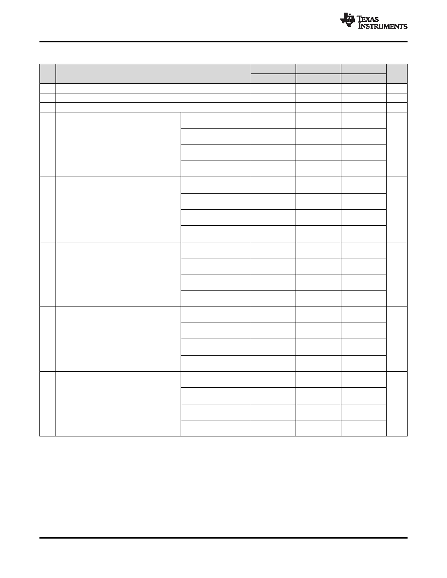
Table 6-73. General Timing Requirements for SPI1 Slave Modes(1)
1.3V, 1.2V
1.1V
1.0V
NO.
UNIT
MIN
MAX
MIN
MAX
MIN
MAX
9
tc(SPC)S
Cycle Time, SPI1_CLK, All Slave Modes
40(2)
50(2)
60(2)
ns
10
tw(SPCH)S
Pulse Width High, SPI1_CLK, All Slave Modes
18
22
27
ns
11
tw(SPCL)S
Pulse Width Low, SPI1_CLK, All Slave Modes
18
22
27
ns
Polarity = 0, Phase = 0,
2P
to SPI1_CLK rising
Polarity = 0, Phase = 1,
Setup time, transmit data
2P
to SPI1_CLK rising
written to SPI before initial
12
tsu(SOMI_SPC)S
ns
clock edge from
Polarity = 1, Phase = 0,
2P
master.(3) (4)
to SPI1_CLK falling
Polarity = 1, Phase = 1,
2P
to SPI1_CLK falling
Polarity = 0, Phase = 0,
15
17
19
from SPI1_CLK rising
Polarity = 0, Phase = 1,
15
17
19
Delay, subsequent bits valid
from SPI1_CLK falling
13
td(SPC_SOMI)S
on SPI1_SOMI after transmit
ns
Polarity = 1, Phase = 0,
edge of SPI1_CLK
15
17
19
from SPI1_CLK falling
Polarity = 1, Phase = 1,
15
17
19
from SPI1_CLK rising
Polarity = 0, Phase = 0,
0.5S-4
0.5S-10
0.5S-12
from SPI1_CLK falling
Polarity = 0, Phase = 1,
0.5S-4
0.5S-10
0.5S-12
Output hold time, SPI1_SOMI
from SPI1_CLK rising
14
toh(SPC_SOMI)S
valid after receive edge of
ns
Polarity = 1, Phase = 0,
SPI1_CLK
0.5S-4
0.5S-10
0.5S-12
from SPI1_CLK rising
Polarity = 1, Phase = 1,
0.5S-4
0.5S-10
0.5S-12
from SPI1_CLK falling
Polarity = 0, Phase = 0,
1.5
to SPI1_CLK falling
Polarity = 0, Phase = 1,
1.5
Input Setup Time, SPI1_SIMO to SPI1_CLK rising
15
tsu(SIMO_SPC)S
valid before receive edge of
ns
Polarity = 1, Phase = 0,
SPI1_CLK
1.5
to SPI1_CLK rising
Polarity = 1, Phase = 1,
1.5
to SPI1_CLK falling
Polarity = 0, Phase = 0,
4
5
6
from SPI1_CLK falling
Polarity = 0, Phase = 1,
4
5
6
Input Hold Time, SPI1_SIMO
from SPI1_CLK rising
16
tih(SPC_SIMO)S
valid after receive edge of
ns
Polarity = 1, Phase = 0,
SPI1_CLK
4
5
6
from SPI1_CLK rising
Polarity = 1, Phase = 1,
4
5
6
from SPI1_CLK falling
(1)
P = SYSCLK2 period; S = tc(SPC)S (SPI slave bit clock period)
(2)
This timing is limited by the timing shown or 3P, whichever is greater.
(3)
First bit may be MSB or LSB depending upon SPI configuration. SO(0) refers to first bit and SO(n) refers to last bit output on
SPI1_SOMI. SI(0) refers to the first bit input and SI(n) refers to the last bit input on SPI1_SIMO.
(4)
Measured from the termination of the write of new data to the SPI module, In analyzing throughput requirements, additional internal bus
cycles must be accounted for to allow data to be written to the SPI module by the CPU.
162
Peripheral Information and Electrical Specifications
Copyright 2010–2014, Texas Instruments Incorporated
Product Folder Links: AM1808
相关PDF资料 |
PDF描述 |
|---|---|
| AM1808BZWTD4 | IC ARM9 CORTEX MCU 361NFBGA |
| AM1808BZCE3 | IC ARM9 CORTEX MCU 361NFBGA |
| AMC60DRTN-S93 | CONN EDGECARD 120PS DIP .100 SLD |
| AMC60DRTH-S93 | CONN EDGECARD 120PS DIP .100 SLD |
| IDT71V65803S100BGGI | IC SRAM 9MBIT 100MHZ 119BGA |
相关代理商/技术参数 |
参数描述 |
|---|---|
| AM1808BZCEA3 | 功能描述:微处理器 - MPU ARM MicroProc RoHS:否 制造商:Atmel 处理器系列:SAMA5D31 核心:ARM Cortex A5 数据总线宽度:32 bit 最大时钟频率:536 MHz 程序存储器大小:32 KB 数据 RAM 大小:128 KB 接口类型:CAN, Ethernet, LIN, SPI,TWI, UART, USB 工作电源电压:1.8 V to 3.3 V 最大工作温度:+ 85 C 安装风格:SMD/SMT 封装 / 箱体:FBGA-324 |
| AM1808BZCEA4 | 制造商:TI 制造商全称:Texas Instruments 功能描述:AM1808 ARM Microprocessor |
| AM1808BZCED3 | 制造商:TI 制造商全称:Texas Instruments 功能描述:AM1808 ARM Microprocessor |
| AM1808BZCED4 | 功能描述:微处理器 - MPU ARM MicroProc RoHS:否 制造商:Atmel 处理器系列:SAMA5D31 核心:ARM Cortex A5 数据总线宽度:32 bit 最大时钟频率:536 MHz 程序存储器大小:32 KB 数据 RAM 大小:128 KB 接口类型:CAN, Ethernet, LIN, SPI,TWI, UART, USB 工作电源电压:1.8 V to 3.3 V 最大工作温度:+ 85 C 安装风格:SMD/SMT 封装 / 箱体:FBGA-324 |
| AM1808BZWT3 | 功能描述:微处理器 - MPU ARM MicroProc RoHS:否 制造商:Atmel 处理器系列:SAMA5D31 核心:ARM Cortex A5 数据总线宽度:32 bit 最大时钟频率:536 MHz 程序存储器大小:32 KB 数据 RAM 大小:128 KB 接口类型:CAN, Ethernet, LIN, SPI,TWI, UART, USB 工作电源电压:1.8 V to 3.3 V 最大工作温度:+ 85 C 安装风格:SMD/SMT 封装 / 箱体:FBGA-324 |
发布紧急采购,3分钟左右您将得到回复。