- 您现在的位置:买卖IC网 > PDF目录375300 > AM29F017D-150F4E (SPANSION LLC) 16 Megabit (2 M x 8-Bit) CMOS 5.0 Volt-only, Uniform Sector Flash Memory PDF资料下载
参数资料
| 型号: | AM29F017D-150F4E |
| 厂商: | SPANSION LLC |
| 元件分类: | DRAM |
| 英文描述: | 16 Megabit (2 M x 8-Bit) CMOS 5.0 Volt-only, Uniform Sector Flash Memory |
| 中文描述: | 2M X 8 FLASH 5V PROM, 150 ns, PDSO40 |
| 封装: | MO-142CD, TSOP-40 |
| 文件页数: | 10/44页 |
| 文件大小: | 1021K |
| 代理商: | AM29F017D-150F4E |
第1页第2页第3页第4页第5页第6页第7页第8页第9页当前第10页第11页第12页第13页第14页第15页第16页第17页第18页第19页第20页第21页第22页第23页第24页第25页第26页第27页第28页第29页第30页第31页第32页第33页第34页第35页第36页第37页第38页第39页第40页第41页第42页第43页第44页
Am29F017D
9
DEVICE BUS OPERATIONS
This section describes the requirements and use of the
device bus operations, which are initiated through the
internal command register. The command register it-
self does not occupy any addressable memory loca-
tion. The register is composed of latches that store the
commands, along with the address and data informa-
tion needed to execute the command. The contents of
the register serve as inputs to the internal state ma-
chine. The state machine outputs dictate the function of
the device. The appropriate device bus operations
table lists the inputs and control levels required, and the
resulting output. The following subsections describe
each of these operations in further detail.
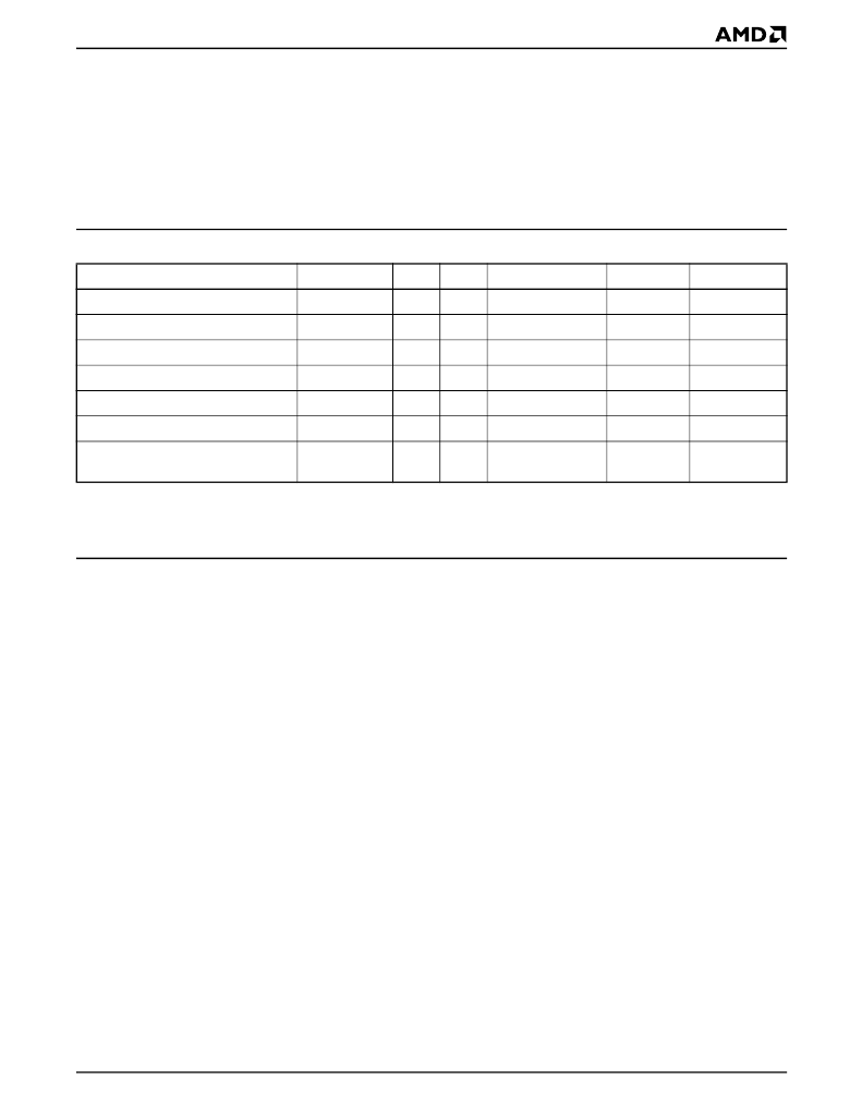
Table 1.
Am29F017D Device Bus Operations
Legend:
L = Logic Low = V
IL
, H = Logic High = V
IH
, V
ID
= 12.0
±
0.5 V, X = Don’t Care, D
IN
= Data In, D
OUT
= Data Out, A
IN
= Address In
Note:
See the sections Sector Group Protection and Temporary Sector Unprotect for more information.
Requirements for Reading Array Data
To read array data from the outputs, the system must
drive the CE# and OE# pins to V
IL
. CE# is the power
control and selects the device. OE# is the output control
and gates array data to the output pins. WE# should re-
main at V
IH
.
The internal state machine is set for reading array
data upon device power-up, or after a hardware reset.
This ensures that no spurious alteration of the mem-
ory content occurs during the power transition. No
command is necessary in this mode to obtain array
data. Standard microprocessor read cycles that as-
sert valid addresses on the device address inputs
produce valid data on the device data outputs. The
device remains enabled for read access until the
command register contents are altered.
See “Reading Array Data” for more information. Refer
to the AC Read Operations table for timing specifica-
tions and to the Read Operations Timings diagram for
the timing waveforms. I
CC1
in the DC Characteristics
table represents the active current specification for
reading array data.
Writing Commands/Command Sequences
To write a command or command sequence (which in-
cludes programming data to the device and erasing
sectors of memory), the system must drive WE# and
CE# to V
IL
, and OE# to V
IH
.
An erase operation can erase one sector, multiple sec-
tors, or the entire device. The Sector Address Tables in-
dicate the address space that each sector occupies. A
“sector address” consists of the address bits required
to uniquely select a sector. See the “Command Defini-
tions” section for details on erasing a sector or the en-
tire chip, or suspending/resuming the erase operation.
After the system writes the autoselect command se-
quence, the device enters the autoselect mode. The
system can then read autoselect codes from the inter-
nal register (which is separate from the memory array)
on DQ7–DQ0. Standard read cycle timings apply in this
mode. Refer to the “Autoselect Mode” and “Autoselect
Command Sequence” sections for more information.
I
CC2
in the DC Characteristics table represents the ac-
tive current specification for the write mode. The “AC
Characteristics” section contains timing specification
tables and timing diagrams for write operations.
Program and Erase Operation Status
During an erase or program operation, the system may
check the status of the operation by reading the status
bits on DQ7–DQ0. Standard read cycle timings and I
CC
Operation
CE#
OE#
WE#
RESET#
A0–A20
DQ0–DQ7
Read
L
L
H
H
A
IN
D
OUT
Write
L
H
L
H
A
IN
D
IN
CMOS Standby
V
CC
± 0.5 V
X
X
V
CC
± 0.5 V
X
High-Z
TTL Standby
H
X
X
H
X
High-Z
Output Disable
L
H
H
H
X
High-Z
Hardware Reset
X
X
X
L
X
High-Z
Temporary Sector Unprotect
(See Note)
X
X
X
V
ID
A
IN
D
IN
相关PDF资料 |
PDF描述 |
|---|---|
| AM29F017D-150F4I | CAT 5E PATCH CORD, BLACK 7 FT. |
| AM29F017D-150FC | CAT 5E PATCH CORD, BLACK 10FT |
| AM29F017D-90E4C | 16 Megabit (2 M x 8-Bit) CMOS 5.0 Volt-only, Uniform Sector Flash Memory |
| AM29F017D-90E4I | 16 Megabit (2 M x 8-Bit) CMOS 5.0 Volt-only, Uniform Sector Flash Memory |
| AM29F017D-70 | 16 Megabit (2 M x 8-Bit) CMOS 5.0 Volt-only, Uniform Sector Flash Memory |
相关代理商/技术参数 |
参数描述 |
|---|---|
| AM29F017D-70FI | 制造商:Spansion 功能描述:FLASH PARALLEL 5V 16MBIT 2MX8 70NS 48TSOP - Trays |
| am29f017d-90fc/t | 制造商:Advanced Micro Devices 功能描述: |
| AM29F032B-120ED | 制造商:Spansion 功能描述: |
| AM29F032B75ED | 制造商:Advanced Micro Devices 功能描述: |
| AM29F032B-75EF | 制造商:Spansion 功能描述: 制造商:Spansion 功能描述:32M (4M X 8-BIT) 5V FLSH SCTR 制造商:Spansion 功能描述:IC, FLASH MEM, 32MBIT, 75NS, 40-TSOP, Memory Type:Flash - NOR, Memory Size:32Mbi |
发布紧急采购,3分钟左右您将得到回复。