- 您现在的位置:买卖IC网 > PDF目录166216 > AM29PDL127H85PCIN (Spansion Inc.) 128 Megabit (8 M x 16-Bit) CMOS 3.0 Volt-only, Page Mode Simultaneous Read/Write Flash Memory with Enhanced VersatileIO Control PDF资料下载
参数资料
| 型号: | AM29PDL127H85PCIN |
| 厂商: | Spansion Inc. |
| 英文描述: | 128 Megabit (8 M x 16-Bit) CMOS 3.0 Volt-only, Page Mode Simultaneous Read/Write Flash Memory with Enhanced VersatileIO Control |
| 中文描述: | 128兆位(8米× 16位),3.0伏的CMOS只,页面模式同步读/写闪存与增强VersatileIO控制记忆 |
| 文件页数: | 33/68页 |
| 文件大小: | 750K |
| 代理商: | AM29PDL127H85PCIN |
第1页第2页第3页第4页第5页第6页第7页第8页第9页第10页第11页第12页第13页第14页第15页第16页第17页第18页第19页第20页第21页第22页第23页第24页第25页第26页第27页第28页第29页第30页第31页第32页当前第33页第34页第35页第36页第37页第38页第39页第40页第41页第42页第43页第44页第45页第46页第47页第48页第49页第50页第51页第52页第53页第54页第55页第56页第57页第58页第59页第60页第61页第62页第63页第64页第65页第66页第67页第68页
June 30, 2003
Am29PDL127H
37
ADV ANCE
I N FO RMAT I O N
data from the non-erasing bank. The system can de-
termine the status of the erase operation by reading
DQ7, DQ6, DQ2, or RY/BY# in the erasing bank.
Refer to the Write Operation Status section for infor-
mation on these status bits.
Once the sector erase operation has begun, only the
Erase Suspend command is valid. All other com-
mands are ignored. However, note that a hardware
reset immediately terminates the erase operation. If
that occurs, the sector erase command sequence
should be reinitiated once that bank has returned to
reading array data, to ensure data integrity.
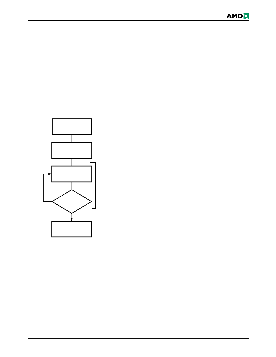
Figure 5 illustrates the algorithm for the erase opera-
tion. Refer to the Erase and Program Operations ta-
bles in the AC Characteristics section for parameters,
and Figure 17 section for timing diagrams.
Figure 5.
Erase Operation
Erase Suspend/Erase Resume
Commands
The Erase Suspend command, B0h, allows the sys-
tem to interrupt a sector erase operation and then read
data from, or program data to, any sector not selected
for erasure. The bank address is required when writing
this command. This command is valid only during the
sector erase operation, including the 80 s time-out
period during the sector erase command sequence.
The Erase Suspend command is ignored if written dur-
ing the chip erase operation or Embedded Program
algorithm.
When the Erase Suspend command is written during
the sector erase operation, the device requires a max-
imum of 20 s to suspend the erase operation. How-
ever, when the Erase Suspend command is written
during the sector erase time-out, the device immedi-
ately terminates the time-out period and suspends the
erase operation. Addresses are “don’t-cares” when
writing the Erase suspend command.
After the erase operation has been suspended, the
bank enters the erase-suspend-read mode. The sys-
tem can read data from or program data to any sector
not selected for erasure. (The device “erase sus-
pends” all sectors selected for erasure.) Reading at
any address within erase-suspended sectors pro-
duces status information on DQ7–DQ0. The system
can use DQ7, or DQ6 and DQ2 together, to determine
if a sector is actively erasing or is erase-suspended.
Refer to the Write Operation Status section for infor-
mation on these status bits.
After an erase-suspended program operation is com-
plete, the bank returns to the erase-suspend-read
mode. The system can determine the status of the
program operation using the DQ7 or DQ6 status bits,
just as in the standard Word Program operation.
Refer to the Write Operation Status section for more
information.
In the erase-suspend-read mode, the system can also
issue the autoselect command sequence. The device
allows reading autoselect codes even at addresses
within erasing sectors, since the codes are not stored
in the memory array. When the device exits the au-
toselect mode, the device reverts to the Erase Sus-
pend mode, and is ready for another valid operation.
Refer to the Autoselect Mode and Autoselect Com-
mand Sequence sections for details.
To resume the sector erase operation, the system
must write the Erase Resume command (address bits
are don’t care). The bank address of the erase-sus-
pended bank is required when writing this command.
Further writes of the Resume command are ignored.
Another Erase Suspend command can be written after
the chip has resumed erasing.
Password Program Command
The Password Program Command permits program-
ming the password that is used as part of the hard-
ware protection scheme. The actual password is
64-bits long. Four Password Program commands are
required to program the password. The system must
enter the unlock cycle, password program command
(38h) and the program address/data for each portion
START
Write Erase
Command Sequence
(Notes 1, 2)
Data Poll to Erasing
Bank from System
Data = FFh?
No
Yes
Erasure Completed
Embedded
Erase
algorithm
in progress
Notes:
1. See Table 13 for erase command sequence.
2. See the section on DQ3 for information on the sector
erase timer.
相关PDF资料 |
PDF描述 |
|---|---|
| AM29PDL127H85VKI | 128 Megabit (8 M x 16-Bit) CMOS 3.0 Volt-only, Page Mode Simultaneous Read/Write Flash Memory with Enhanced VersatileIO Control |
| AM29PDL127H85VKIN | 128 Megabit (8 M x 16-Bit) CMOS 3.0 Volt-only, Page Mode Simultaneous Read/Write Flash Memory with Enhanced VersatileIO Control |
| Am29PDL127H88 | 128 Megabit (8 M x 16-Bit) CMOS 3.0 Volt-only, Page Mode Simultaneous Read/Write Flash Memory with Enhanced VersatileIO Control |
| AM29PDL127H83VKI | 128 Megabit (8 M x 16-Bit) CMOS 3.0 Volt-only, Page Mode Simultaneous Read/Write Flash Memory with Enhanced VersatileIO Control |
| AM29SL800CB-100ED | 512K X 16 FLASH 1.8V PROM, 100 ns, PDSO48 |
相关代理商/技术参数 |
参数描述 |
|---|---|
| AM29PDL128G70RPEI | 制造商:Spansion 功能描述:FLASH PARALLEL 3V/3.3V 128MBIT 8MX16/4M X 32 70NS 80FBGA - Trays |
| AM29PDL128G80PEF | 制造商:Spansion 功能描述:SPZAM29PDL128G80PEF 128M FLASH EOL100409 |
| AM29PL141BXA | 制造商:AMD 功能描述:* |
| AM29PL141DC | 制造商:Advanced Micro Devices 功能描述:USER PROGRAMMABLE SPECIAL FUNCTION ASIC, 28 Pin, DIP |
| AM29PL160CB-90SF | 制造商:Advanced Micro Devices 功能描述: |
发布紧急采购,3分钟左右您将得到回复。