- 您现在的位置:买卖IC网 > PDF目录166216 > AM29PDL127H85PCIN (Spansion Inc.) 128 Megabit (8 M x 16-Bit) CMOS 3.0 Volt-only, Page Mode Simultaneous Read/Write Flash Memory with Enhanced VersatileIO Control PDF资料下载
参数资料
| 型号: | AM29PDL127H85PCIN |
| 厂商: | Spansion Inc. |
| 英文描述: | 128 Megabit (8 M x 16-Bit) CMOS 3.0 Volt-only, Page Mode Simultaneous Read/Write Flash Memory with Enhanced VersatileIO Control |
| 中文描述: | 128兆位(8米× 16位),3.0伏的CMOS只,页面模式同步读/写闪存与增强VersatileIO控制记忆 |
| 文件页数: | 6/68页 |
| 文件大小: | 750K |
| 代理商: | AM29PDL127H85PCIN |
第1页第2页第3页第4页第5页当前第6页第7页第8页第9页第10页第11页第12页第13页第14页第15页第16页第17页第18页第19页第20页第21页第22页第23页第24页第25页第26页第27页第28页第29页第30页第31页第32页第33页第34页第35页第36页第37页第38页第39页第40页第41页第42页第43页第44页第45页第46页第47页第48页第49页第50页第51页第52页第53页第54页第55页第56页第57页第58页第59页第60页第61页第62页第63页第64页第65页第66页第67页第68页
12
Am29PDL127H
June 30, 2003
ADV ANCE
I N FO RMAT I O N
cess has access time of t
ACC or tCE. Here again, CE#
selects the device and OE# is the output control and
should be used to gate data to the output inputs if the
device is selected. Fast page mode accesses are ob-
tained by keeping A22–A3 constant and changing
A2–A0 to select the specific word within that page.
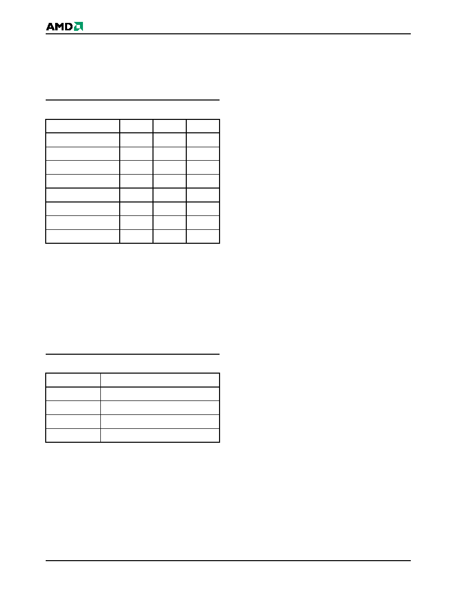
Table 2.
Page Select
Simultaneous Operation
In addition to the conventional features (read, pro-
gram, erase-suspend read, and erase-suspend pro-
gram), the device is capable of reading data from one
bank of memory while a program or erase operation is
in progress in another bank of memory (simultaneous
operation). The bank can be selected by bank ad-
dresses (A22–A20) with zero latency.
The simultaneous operation can execute multi-func-
tion mode in the same bank.
Table 3.
Bank Select
Writing Commands/Command Sequences
To write a command or command sequence (which in-
cludes programming data to the device and erasing
sectors of memory), the system must drive WE# and
CE# to V
IL, and OE# to VIH.
The device features an Unlock Bypass mode to facil-
itate faster programming. Once a bank enters the Un-
lock Bypass mode, only two write cycles are required
to program a word, instead of four. The “Word Pro-
gram Command Sequence” section has details on
programming data to the device using both standard
and Unlock Bypass command sequences.
An erase operation can erase one sector, multiple sec-
tors, or the entire device. Table 4 indicates the address
space that each sector occupies. A “bank address” is
the address bits required to uniquely select a bank.
Similarly, a “sector address” refers to the address bits
required to uniquely select a sector. The “Command
Definitions” section has details on erasing a sector or
the entire chip, or suspending/resuming the erase op-
eration.
I
CC2 in the DC Characteristics table represents the ac-
tive current specification for the write mode. The AC
Characteristics section contains timing specification
tables and timing diagrams for write operations.
Accelerated Program Operation
The device offers accelerated program operations
through the ACC function. This function is primarily in-
tended to allow faster manufacturing throughput at the
factory.
If the system asserts V
HH on this pin, the device auto-
matically enters the aforementioned Unlock Bypass
mode, temporarily unprotects any protected sectors,
and uses the higher voltage on the pin to reduce the
time required for program operations. The system
would use a two-cycle program command sequence
as required by the Unlock Bypass mode. Removing
V
HH from the WP#/ACC pin returns the device to nor-
mal operation. Note that V
HH must not be asserted on
WP#/ACC for operations other than accelerated pro-
gramming, or device damage may result. In addition,
the WP#/ACC pin should be raised to V
CC when not in
use. That is, the WP#/ACC pin should not be left float-
ing or unconnected; inconsistent behavior of the de-
vice may result.
Autoselect Functions
If the system writes the autoselect command se-
quence, the device enters the autoselect mode. The
system can then read autoselect codes from the inter-
nal register (which is separate from the memory array)
on DQ15–DQ0. Standard read cycle timings apply in
this mode. Refer to the Autoselect Mode and Autose-
lect Command Sequence sections for more informa-
tion.
Standby Mode
When the system is not reading or writing to the de-
vice, it can place the device in the standby mode. In
this mode, current consumption is greatly reduced,
and the outputs are placed in the high impedance
state, independent of the OE# input.
The device enters the CMOS standby mode when the
CE# and RESET# pins are both held at V
IO ± 0.3 V.
Word
A2
A1
A0
Word 0
000
Word 1
001
Word 2
010
Word 3
011
Word 4
100
Word 5
101
Word 6
110
Word 7
111
Bank
A22–A20
Bank A
000
Bank B
001, 010, 011
Bank C
100, 101, 110
Bank D
111
相关PDF资料 |
PDF描述 |
|---|---|
| AM29PDL127H85VKI | 128 Megabit (8 M x 16-Bit) CMOS 3.0 Volt-only, Page Mode Simultaneous Read/Write Flash Memory with Enhanced VersatileIO Control |
| AM29PDL127H85VKIN | 128 Megabit (8 M x 16-Bit) CMOS 3.0 Volt-only, Page Mode Simultaneous Read/Write Flash Memory with Enhanced VersatileIO Control |
| Am29PDL127H88 | 128 Megabit (8 M x 16-Bit) CMOS 3.0 Volt-only, Page Mode Simultaneous Read/Write Flash Memory with Enhanced VersatileIO Control |
| AM29PDL127H83VKI | 128 Megabit (8 M x 16-Bit) CMOS 3.0 Volt-only, Page Mode Simultaneous Read/Write Flash Memory with Enhanced VersatileIO Control |
| AM29SL800CB-100ED | 512K X 16 FLASH 1.8V PROM, 100 ns, PDSO48 |
相关代理商/技术参数 |
参数描述 |
|---|---|
| AM29PDL128G70RPEI | 制造商:Spansion 功能描述:FLASH PARALLEL 3V/3.3V 128MBIT 8MX16/4M X 32 70NS 80FBGA - Trays |
| AM29PDL128G80PEF | 制造商:Spansion 功能描述:SPZAM29PDL128G80PEF 128M FLASH EOL100409 |
| AM29PL141BXA | 制造商:AMD 功能描述:* |
| AM29PL141DC | 制造商:Advanced Micro Devices 功能描述:USER PROGRAMMABLE SPECIAL FUNCTION ASIC, 28 Pin, DIP |
| AM29PL160CB-90SF | 制造商:Advanced Micro Devices 功能描述: |
发布紧急采购,3分钟左右您将得到回复。