- 您现在的位置:买卖IC网 > PDF目录378403 > AN-5026 (Fairchild Semiconductor Corporation) Circular Connector; No. of Contacts:19; Series:MS27656; Body Material:Aluminum; Connecting Termination:Crimp; Connector Shell Size:15; Circular Contact Gender:Pin; Circular Shell Style:Wall Mount Receptacle; Insert Arrangement:15-19 RoHS Compliant: No PDF资料下载
参数资料
| 型号: | AN-5026 |
| 厂商: | Fairchild Semiconductor Corporation |
| 元件分类: | 圆形连接器 |
| 英文描述: | Circular Connector; No. of Contacts:19; Series:MS27656; Body Material:Aluminum; Connecting Termination:Crimp; Connector Shell Size:15; Circular Contact Gender:Pin; Circular Shell Style:Wall Mount Receptacle; Insert Arrangement:15-19 RoHS Compliant: No |
| 中文描述: | 使用的BGA封装 |
| 文件页数: | 5/8页 |
| 文件大小: | 722K |
| 代理商: | AN-5026 |
5
www.fairchildsemi.com
A
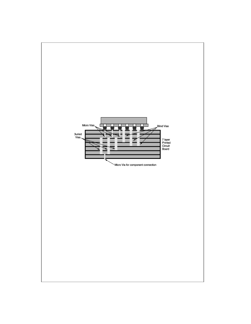
BGA Via Design and Layout Options
(Continued)
Through-board vias are the most economical via type from
a board manufacturing perspective. However, trade-offs in
highly space-constrained designs may be required.
Through-board vias create a matrix of vias on the board
backside, limiting its use for traces and components. These
vias can also disrupt the smooth layout of bus runs on
internal board layers or limit their placement.
With the ever increasing demand for more compact sys-
tems and higher density layouts, three more advanced
methods of via connections are being used, the blind via,
the buried via, and the micro via. Figure 13 shows an
example of these via types used in conjunction with a BGA.
Blind vias connect one side of the board to some inner lay-
ers, but do not run completely through to the other side.
Buried vias connect internal board layers but do not extend
to the exterior of the board.
Micro vias are very small vias (4
μ
m is typical) and can be
used for via in pad layouts. This can significantly reduce via
density, increase routing options on the board, and con-
serve space. Laser technology is often used to drill micro
vias. Lasers drill micro vias through a 4 millimeter thick
dielectric layer, allowing connection to the first internal
layer of the board. Two 4 millimeter layers can be drilled
with a laser, allowing connection from the surface to the
second board layer.
These three via types are more costly than through-board
vias from a manufacturing standpoint. However, there are
two significant advantages over through-board vias; the
elimination of backside vias frees that layer for component
placement, and some internal layers and the backside are
freed up for traces and uninterrupted bus runs.
FIGURE 13. Multi Layer Board with BGA Connections to Micro Vias, Buried Vias and Blind Vias
相关PDF资料 |
PDF描述 |
|---|---|
| AN-5031 | GTLP Power Configuration |
| AN-5058 | Family Frequently Asked Questions (FAQs) |
| AN-5061 | Layout Guidelines |
| AN-53 | Implementing an RC5051 DC-DC Converter on Pentium II Motherboards |
| AN-6003 | Shoot-through in Synchronous Buck Converters |
相关代理商/技术参数 |
参数描述 |
|---|---|
| AN502-6-10 | 制造商:NEW SURPLUS HARDWARE 功能描述: |
| AN5026K | 制造商:PANASONIC 制造商全称:Panasonic Semiconductor 功能描述:REMOTE CONTROL RECEIVING IC |
| AN-5029 | 制造商:FAIRCHILD 制造商全称:Fairchild Semiconductor 功能描述:Interfacing Between PECL and LVDS Differential Technologies |
| AN5031 | 制造商:未知厂家 制造商全称:未知厂家 功能描述:TV Channel Selector Circuit |
| AN-5031 | 制造商:FAIRCHILD 制造商全称:Fairchild Semiconductor 功能描述:GTLP Power Configuration |
发布紧急采购,3分钟左右您将得到回复。