- 您现在的位置:买卖IC网 > PDF目录378403 > AN-7820 (Fairchild Semiconductor Corporation) Circular Connector; No. of Contacts:37; Series:MS27656; Body Material:Aluminum; Connecting Termination:Crimp; Connector Shell Size:15; Circular Contact Gender:Pin; Circular Shell Style:Wall Mount Receptacle; Insert Arrangement:15-35 RoHS Compliant: No PDF资料下载
参数资料
| 型号: | AN-7820 |
| 厂商: | Fairchild Semiconductor Corporation |
| 元件分类: | 圆形连接器 |
| 英文描述: | Circular Connector; No. of Contacts:37; Series:MS27656; Body Material:Aluminum; Connecting Termination:Crimp; Connector Shell Size:15; Circular Contact Gender:Pin; Circular Shell Style:Wall Mount Receptacle; Insert Arrangement:15-35 RoHS Compliant: No |
| 中文描述: | 评价委员会 |
| 文件页数: | 12/17页 |
| 文件大小: | 206K |
| 代理商: | AN-7820 |
12
5/22/97
AN7820/24
DYNAMIC TESTING
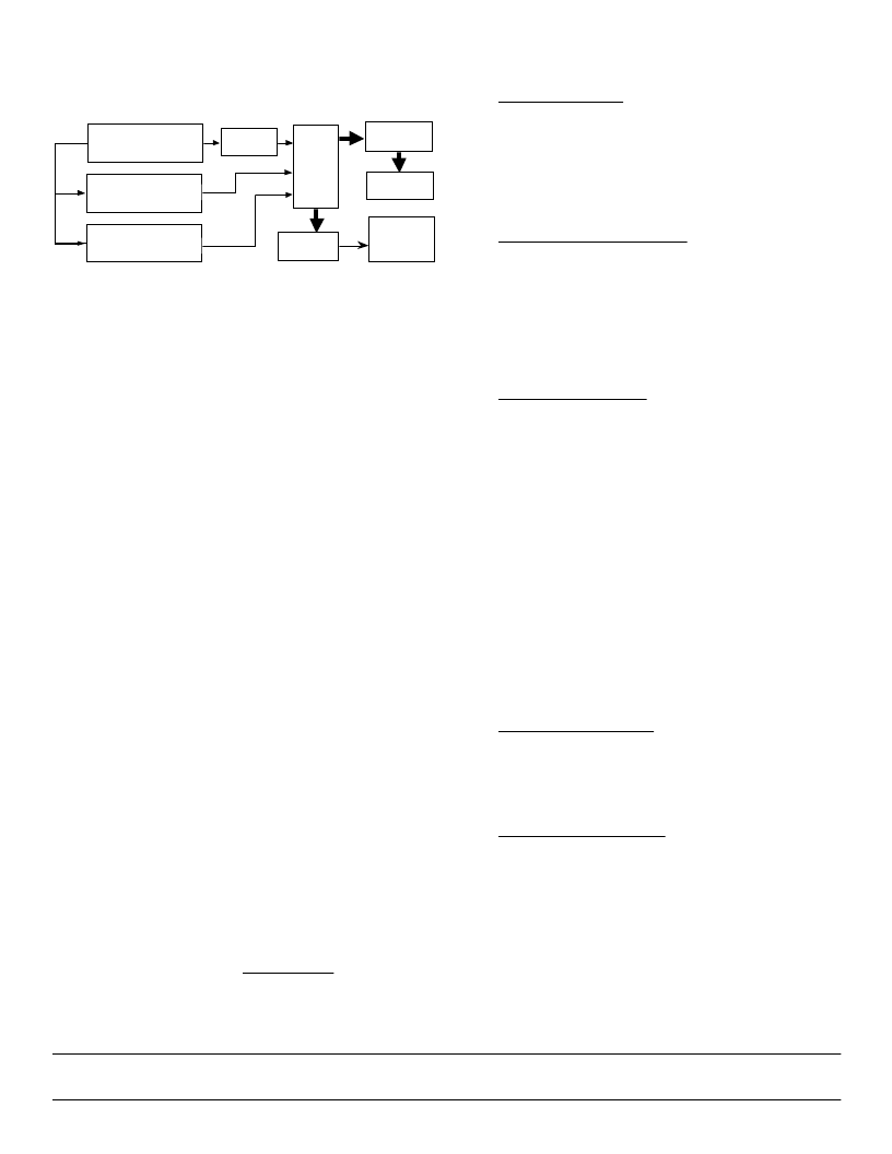
Figure 16: Dynamic Testing Test Set-up
GENERATOR # 1
REF
OUT
O
GENERATOR #2
REF
IN
GENERATOR # 3
REF
IN
BPF
IN
E
C
V
C
P
HIGH SPEED
MEMORY
CPU / DSP
DB792
SCOPE OR
SPECTRUM
ANALYSER
DAC
OUT
O
O
O
P2/P3
Figure 16 is the recommended block diagram for dynamic
testing of the SPT7820 or SPT7824 using the EB7820/24
evaluation board. In earlier tests, the DAC OUT signal was
used to analyze the ADC’s dynamic performances (SNR and
THD) through a spectrum analyzer. This method of testing
presented some uncertainties. The DAC had to be near
perfect and free from glitches, and its dynamic accuracy
(DLE and ILE) had to be far better than the ADC under test.
Any errors in the DAC wereadded to the total SNR and/or
THD.
Today, it is preferable to perform these tests by means of
digital signal processing (DSP). There are currently numer-
ous standard software packages on the market to service
this application. The EB7820/24 provides the data outputs
through P2. (See table 5 for detail.) The reconstruction DAC
can be obtained from DB792 daughter board. Both set-ups
are very important in characterizing the dynamic perfor-
mance of the SPT7820 or SPT7824.
In many cases, the speed of the capture memory is much
slower than the available output valid data of the ADC under
test. In this case, it is necessary to decimate the capture
clock at a rate of Fs/N, where N is a power of 2. The beat
frequency can be achieved by slightly changing the analog
input frequency by an amount of
fin. For a 4096-point FFT,
the beat frequency of
fin = Fc/4096 is added (or subtracted)
to the analog input frequency. 4096 data points are filled in
one test period where the input is at Fin
±
(Fc/4096) and the
output is updated at 1/Fc interval. Select Fin as the multiple
(integer) of Fc to achieve a complete system synchroniza-
tion. Both capture memory and the DAC run at a relatively
low update rate (Fs/N).
The daughter board, DB972, is capable of updating to 80
MSPS.
EB7820/24 CALIBRATION
This section is a guide for the DC calibration of the EB7820/
24 if needed. Note that this board was fully calibrated before
shipment. VST and VSB voltages require new calibration on
each new SPT7820 or 7824.
Check for installation of jumpers SJ2B, SJ2C and SJ3.
1.0
1.1
Equipment Needed
Four DC power supplies: analog +5 V, analog -5.2 V,
digital +5 V and digital -5.2 V.
One Hewlett Packard, HP3325A, function generator or
equivalent.
One DVM with 5 and 1/2 digit precision.
One Oscilloscope.
1.2
1.3
1.4
2.0
2.1
Equipment Set-Up / Hook-Up
Ensure that socket U1 does not haveSPT7820 or
SPT7824 in it.
Connect all four power supplies as shown in table 1,
and figures 2 and figure 3.
Connect the function generator to CLK BNC.
Set the CLK to 3 MHz, sine wave ,
±
2 V.
Connect VIN to AGND.
2.2
2.3
2.4
2.5
3.0
3.1
3.2
3.3
3.4
3.5
3.6
References Calibration
Monitor TP1 with respect to AGND test point with DVM.
Adjust R1 for +2.500 V at TP1.
Monitor TP2 with respect to AGND test point with DVM.
Adjust R2 for -2.500 V at TP2.
Turn all power to off.
Install SPT7820 or SPT7824 into U1 socket. (Fepeat
from this procedure for all new devices.)
Turn all power back to on.
Monitor U1, pin 22 (VST) with respect to AGND test
point with DVM.
Adjust R1 for +2.000 V at VST.
3.10 Monitor U1, pin 27 (VSB) with respect to AGND test
point with DVM.
3.11 Adjust R2 for -2.000 V at VSB.
3.12 Repeat the procedure from paragraph 3.8 until VST
and VSB reach the desired voltages (
±
2.000 V respec-
tively).
3.7
3.8
3.9
4.0
4.1
Clock Circuit Calibration
Monitor PJ1 with scope on channel 1 (externally sync
to the generator).
Observe the TTL clock and adjust R3 for approximately
50% of duty cycle.
4.2
5.0
5.1
5.2
5.3
Latches (U7 and U8) Test
Remove R10.
Connect VIN to TP1.
Monitor P2, odd number pins (7-25), with scope and
observe TTL-logic high on all pins.
Connect VIN to TP2 .
Monitor P2, odd number pins (7-25), with scope and
observe TTL logic low on all pins.
5.4
5.5
End of calibration Procedure
相关PDF资料 |
PDF描述 |
|---|---|
| AN-9008 | Circular Connector; No. of Contacts:37; Series:MS27656; Body Material:Aluminum; Connecting Termination:Crimp; Connector Shell Size:15; Circular Contact Gender:Socket; Circular Shell Style:Wall Mount Receptacle RoHS Compliant: No |
| AN-902 | Twisted Pair FDDI Magnetics Overview and Recommendations |
| AN-90 | 74C Family Characteristics |
| AN-994-1 | MAXIMIZING THE EFFECTIVENESS OF YOUR SMD ASSEMBLIES |
| AN-CC1002 | Design Considerations for ISD1700 Family |
相关代理商/技术参数 |
参数描述 |
|---|---|
| AN7820F | 制造商:PANASONIC 制造商全称:Panasonic Semiconductor 功能描述:3-pin positive output voltage regulator (1 A type) |
| AN7824 | 制造商:Panasonic Industrial Company 功能描述:IC |
| AN7824F | 制造商:PANASONIC 制造商全称:Panasonic Semiconductor 功能描述:3-pin positive output voltage regulator (1 A type) |
| AN783-6 | 制造商: 功能描述: |
| AN783-6D | 制造商: 功能描述: 制造商:undefined 功能描述: |
发布紧急采购,3分钟左右您将得到回复。