参数资料
| 型号: | APA1000-CGS624B |
| 厂商: | Microsemi SoC |
| 文件页数: | 99/178页 |
| 文件大小: | 0K |
| 描述: | IC FPGA PROASIC+ 1M 624-CGA |
| 标准包装: | 1 |
| 系列: | ProASICPLUS |
| RAM 位总计: | 202752 |
| 输入/输出数: | 440 |
| 门数: | 1000000 |
| 电源电压: | 2.3 V ~ 2.7 V |
| 安装类型: | 通孔 |
| 封装/外壳: | 624-BCCGA |
| 供应商设备封装: | 624-CCGA(32.5x32.5) |
第1页第2页第3页第4页第5页第6页第7页第8页第9页第10页第11页第12页第13页第14页第15页第16页第17页第18页第19页第20页第21页第22页第23页第24页第25页第26页第27页第28页第29页第30页第31页第32页第33页第34页第35页第36页第37页第38页第39页第40页第41页第42页第43页第44页第45页第46页第47页第48页第49页第50页第51页第52页第53页第54页第55页第56页第57页第58页第59页第60页第61页第62页第63页第64页第65页第66页第67页第68页第69页第70页第71页第72页第73页第74页第75页第76页第77页第78页第79页第80页第81页第82页第83页第84页第85页第86页第87页第88页第89页第90页第91页第92页第93页第94页第95页第96页第97页第98页当前第99页第100页第101页第102页第103页第104页第105页第106页第107页第108页第109页第110页第111页第112页第113页第114页第115页第116页第117页第118页第119页第120页第121页第122页第123页第124页第125页第126页第127页第128页第129页第130页第131页第132页第133页第134页第135页第136页第137页第138页第139页第140页第141页第142页第143页第144页第145页第146页第147页第148页第149页第150页第151页第152页第153页第154页第155页第156页第157页第158页第159页第160页第161页第162页第163页第164页第165页第166页第167页第168页第169页第170页第171页第172页第173页第174页第175页第176页第177页第178页
ProASICPLUS Flash Family FPGAs
v5.9
2-17
Logic Tile Timing Characteristics
Timing characteristics for ProASICPLUS devices fall into
three categories: family dependent, device dependent,
and design dependent. The input and output buffer
characteristics are common to all ProASICPLUS family
members. Internal routing delays are device dependent.
Design dependency means that actual delays are not
determined until after placement and routing of the
user’s design are complete. Delay values may then be
determined by using the Timer utility or by performing
simulation with post-layout delays.
Critical Nets and Typical Nets
Propagation delays are expressed only for typical nets,
which are used for initial design performance evaluation.
Critical net delays can then be applied to the most
timing-critical paths. Critical nets are determined by net
property assignment prior to place-and-route. Refer to
the Actel Designer User’s Guide or online help for details
on using constraints.
Timing Derating
Since ProASICPLUS devices are manufactured with a
CMOS process, device performance will vary with
temperature, voltage, and process. Minimum timing
parameters
reflect
maximum
operating
voltage,
minimum operating temperature, and optimal process
variations. Maximum timing parameters reflect minimum
operating voltage, maximum operating temperature,
and
worst-case
process
variations
(within
process
specifications). The derating factors shown in Table 2-9
should be applied to all timing data contained within
this datasheet.
All timing numbers listed in this datasheet represent
sample timing characteristics of ProASICPLUS devices.
Actual timing delay values are design-specific and can be
derived from the Timer tool in Actel’s Designer software
after place-and-route.
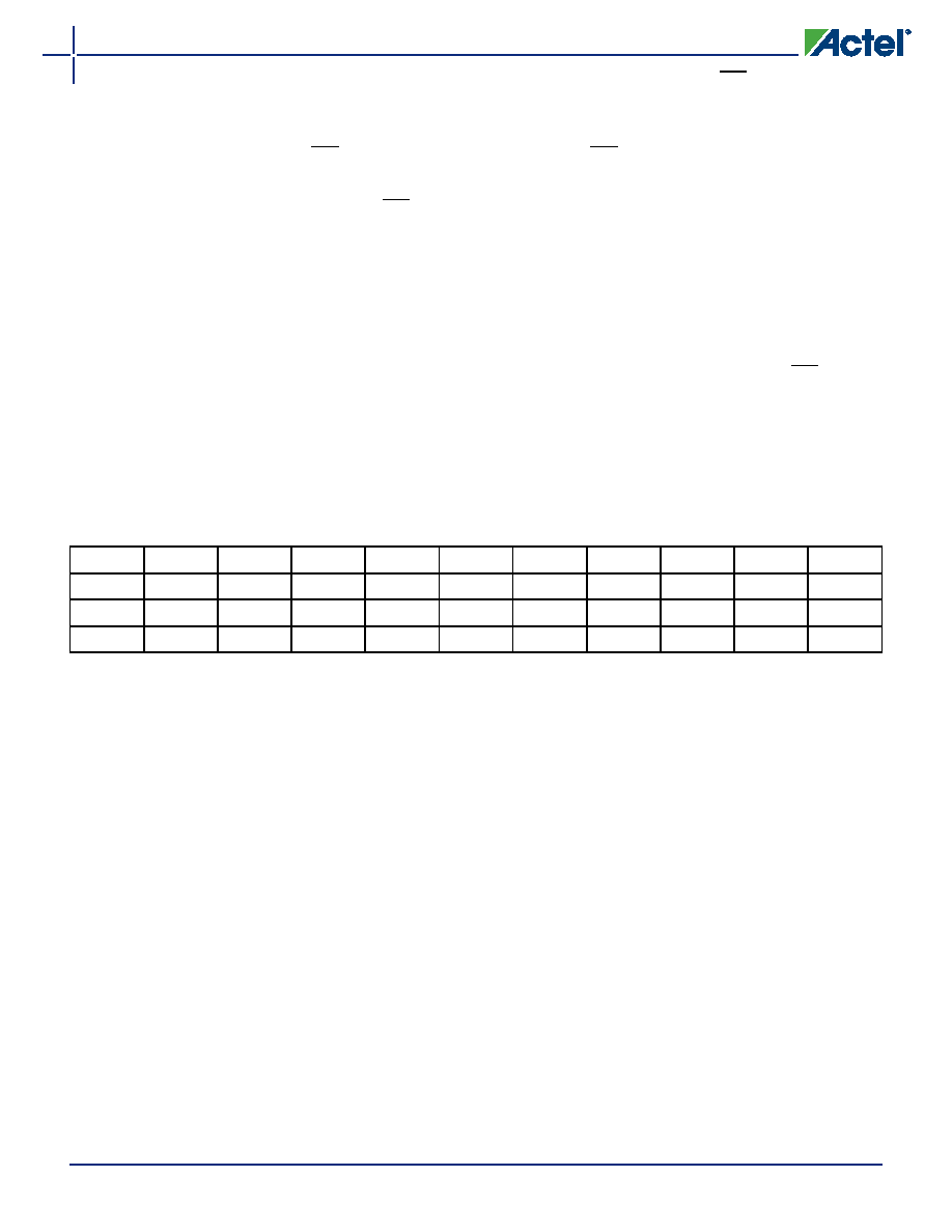
Table 2-9
Temperature and Voltage Derating Factors
(Normalized to Worst-Case Commercial, TJ = 70°C, VDD = 2.3 V)
–55°C
–40°C
0°C
25°C
70°C
85°C
110°C
125°C
135°C
150°C
2.3 V
0.84
0.860.910.941.001.021.05
1.13
1.181.27
2.5 V
0.81
0.820.870.900.950.981.01
1.09
1.131.21
2.7 V
0.77
0.790.830.860.910.930.96
1.04
1.081.16
Notes:
1. The user can set the junction temperature in Designer software to be any integer value in the range of –55°C to 175°C.
2. The user can set the core voltage in Designer software to be any value between 1.4 V and 1.6 V.
相关PDF资料 |
PDF描述 |
|---|---|
| AS1747-BTDT | IC SWITCH DUAL SPDT 10-TDFN |
| AS1753V-T | IC SWITCH QUAD SPST 16TQFN |
| AS2522B-T | IC LINE INTERFACE TELEPH 32-TQFP |
| AS2522B | IC LINE INTERFACE TELEPH 32-TQFP |
| AS2524-T | IC LINE INTERFACE/SPKRPH 28-SOIC |
相关代理商/技术参数 |
参数描述 |
|---|---|
| APA1000-CGS624M | 制造商:Microsemi Corporation 功能描述:FPGA ProASICPLUS Family 1M Gates 180MHz 0.22um Technology 2.5V 624-Pin CCGA 制造商:Microsemi Corporation 功能描述:APA1000-CGS624M - Trays 制造商:Microsemi Corporation 功能描述:IC FPGA PROASIC+ 1M 624CCGA |
| APA1000-CQ208B | 功能描述:IC FPGA PROASIC+ 1M 208-CQFP RoHS:否 类别:集成电路 (IC) >> 嵌入式 - FPGA(现场可编程门阵列) 系列:ProASICPLUS 标准包装:40 系列:Spartan® 6 LX LAB/CLB数:3411 逻辑元件/单元数:43661 RAM 位总计:2138112 输入/输出数:358 门数:- 电源电压:1.14 V ~ 1.26 V 安装类型:表面贴装 工作温度:-40°C ~ 100°C 封装/外壳:676-BGA 供应商设备封装:676-FBGA(27x27) |
| APA1000-CQ208M | 制造商:Microsemi Corporation 功能描述:FPGA ProASICPLUS Family 1M Gates 180MHz 0.22um Technology 2.5V 208-Pin CQFP 制造商:Microsemi Corporation 功能描述:FPGA PROASICPLUS 1M GATES 180MHZ 0.22UM 2.5V 208CQFP - Trays |
| APA1000-CQ352B | 功能描述:IC FPGA PROASIC+ 1M 352-CQFP RoHS:否 类别:集成电路 (IC) >> 嵌入式 - FPGA(现场可编程门阵列) 系列:ProASICPLUS 标准包装:40 系列:Spartan® 6 LX LAB/CLB数:3411 逻辑元件/单元数:43661 RAM 位总计:2138112 输入/输出数:358 门数:- 电源电压:1.14 V ~ 1.26 V 安装类型:表面贴装 工作温度:-40°C ~ 100°C 封装/外壳:676-BGA 供应商设备封装:676-FBGA(27x27) |
| APA1000-CQ352M | 制造商:Microsemi Corporation 功能描述:FPGA ProASICPLUS Family 1M Gates 180MHz 0.22um Technology 2.5V 352-Pin CQFP 制造商:Microsemi Corporation 功能描述:FPGA PROASICPLUS 1M GATES 180MHZ 0.22UM 2.5V 352CQFP - Trays |
发布紧急采购,3分钟左右您将得到回复。