参数资料
| 型号: | APA450-BGG456I |
| 厂商: | Microsemi SoC |
| 文件页数: | 152/178页 |
| 文件大小: | 0K |
| 描述: | IC FPGA PROASIC+ 450K 456-PBGA |
| 标准包装: | 24 |
| 系列: | ProASICPLUS |
| RAM 位总计: | 110592 |
| 输入/输出数: | 344 |
| 门数: | 450000 |
| 电源电压: | 2.3 V ~ 2.7 V |
| 安装类型: | 表面贴装 |
| 工作温度: | -40°C ~ 85°C |
| 封装/外壳: | 456-BBGA |
| 供应商设备封装: | 456-PBGA(35x35) |
第1页第2页第3页第4页第5页第6页第7页第8页第9页第10页第11页第12页第13页第14页第15页第16页第17页第18页第19页第20页第21页第22页第23页第24页第25页第26页第27页第28页第29页第30页第31页第32页第33页第34页第35页第36页第37页第38页第39页第40页第41页第42页第43页第44页第45页第46页第47页第48页第49页第50页第51页第52页第53页第54页第55页第56页第57页第58页第59页第60页第61页第62页第63页第64页第65页第66页第67页第68页第69页第70页第71页第72页第73页第74页第75页第76页第77页第78页第79页第80页第81页第82页第83页第84页第85页第86页第87页第88页第89页第90页第91页第92页第93页第94页第95页第96页第97页第98页第99页第100页第101页第102页第103页第104页第105页第106页第107页第108页第109页第110页第111页第112页第113页第114页第115页第116页第117页第118页第119页第120页第121页第122页第123页第124页第125页第126页第127页第128页第129页第130页第131页第132页第133页第134页第135页第136页第137页第138页第139页第140页第141页第142页第143页第144页第145页第146页第147页第148页第149页第150页第151页当前第152页第153页第154页第155页第156页第157页第158页第159页第160页第161页第162页第163页第164页第165页第166页第167页第168页第169页第170页第171页第172页第173页第174页第175页第176页第177页第178页
ProASICPLUS Flash Family FPGAs
v5.9
2-65
Asynchronous FIFO Full and Empty Transitions
The asynchronous FIFO accepts writes and reads while
not full or not empty. When the FIFO is full, all writes are
inhibited. Conversely, when the FIFO is empty, all reads
are inhibited. A problem is created if the FIFO is written
to during the transition from full to not full, or read
during the transition from empty to not empty. The
exact time at which the write or read operation changes
from inhibited to accepted after the read (write) signal
which causes the transition from full or empty to not full
or not empty is indeterminate. For slow cycles, this
indeterminate period starts 1 ns after the RB (WB)
transition, which deactivates full or not empty and ends
3 ns after the RB (WB) transition. For fast cycles, the
indeterminate period ends 3 ns (7.5 ns – RDL (WRL)) after
the RB (WB) transition, whichever is later (Table 2-1 on
page 2-4).
The timing diagram for write is shown in Figure 2-35 on
page 2-62. The timing diagram for read is shown in
Figure 2-36 on page 2-63. For basic SRAM configurations,
see Table 2-14 on page 2-22. When reset is asserted, the
empty flag will be asserted, the counters will reset, the
outputs go to zero, but the internal RAM is not erased.
Enclosed Timing Diagrams – FIFO Mode:
The following timing diagrams apply only to single cell;
they are not applicable to cascaded cells. For more
information, refer to the ProASICPLUS RAM/FIFO Blocks
application note.
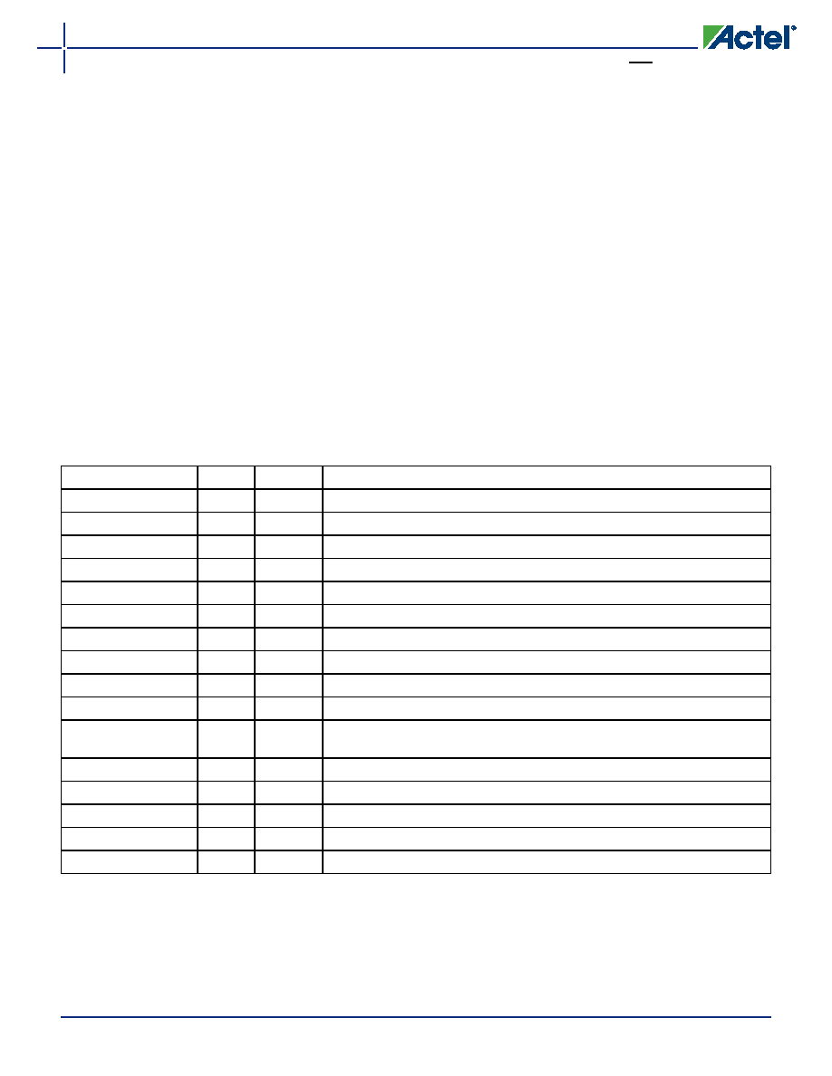
Table 2-62 Memory Block FIFO Interface Signals
FIFO Signal
Bits
In/Out
Description
WCLKS
1
In
Write clock used for synchronization on write side
RCLKS
1
In
Read clock used for synchronization on read side
LEVEL [0:7]*
8
In
Direct configuration implements static flag logic
RBLKB
1
In
Read block select (active Low)
RDB
1
In
Read pulse (active Low)
RESET
1
In
Reset for FIFO pointers (active Low)
WBLKB
1
In
Write block select (active Low)
DI[0:8]
9
In
Input data bits [0:8], [8] will be generated if PARGEN is true
WRB
1
In
Write pulse (active Low)
FULL, EMPTY
2
Out
FIFO flags. FULL prevents write and EMPTY prevents read
EQTH, GEQTH*
2
Out
EQTH is true when the FIFO holds the number of words specified by the LEVEL signal.
GEQTH is true when the FIFO holds (LEVEL) words or more
DO[0:8]
9
Out
Output data bits [0:8]
RPE
1
Out
Read parity error (active High)
WPE
1
Out
Write parity error (active High)
LGDEP [0:2]
3
In
Configures DEPTH of the FIFO to 2 (LGDEP+1)
PARODD
1
In
Selects Odd parity generation/detect when high, Even when low
Note: *LEVEL is always eight bits (0000.0000, 0000.0001). That means for values of DEPTH greater than 256, not all values will be
possible, e.g. for DEPTH = 512, the LEVEL can only have the values 2, 4, . . ., 512. The LEVEL signal circuit will generate signals that
indicate whether the FIFO is exactly filled to the value of LEVEL (EQTH) or filled equal or higher (GEQTH) than the specified LEVEL.
Since counting starts at 0, EQTH will become true when the FIFO holds (LEVEL+1) words for 512-bit FIFOs.
相关PDF资料 |
PDF描述 |
|---|---|
| A54SX72A-1PQG208I | IC FPGA SX-A 108K 208-PQFP |
| A54SX72A-1PQ208I | IC FPGA SX-A 108K 208-PQFP |
| A54SX72A-2PQ208 | IC FPGA SX-A 108K 208-PQFP |
| A54SX72A-2PQG208 | IC FPGA SX-A 108K 208-PQFP |
| 10320-A200-00 | CONN JUNCTION SHELL 20POS STRGT |
相关代理商/技术参数 |
参数描述 |
|---|---|
| APA450-BGGB | 制造商:ACTEL 制造商全称:Actel Corporation 功能描述:ProASIC Flash Family FPGAs |
| APA450-BGGES | 制造商:ACTEL 制造商全称:Actel Corporation 功能描述:ProASIC Flash Family FPGAs |
| APA450-BGGI | 制造商:ACTEL 制造商全称:Actel Corporation 功能描述:ProASIC Flash Family FPGAs |
| APA450-BGGM | 制造商:ACTEL 制造商全称:Actel Corporation 功能描述:ProASIC Flash Family FPGAs |
| APA450-BGGPP | 制造商:ACTEL 制造商全称:Actel Corporation 功能描述:ProASIC Flash Family FPGAs |
发布紧急采购,3分钟左右您将得到回复。