参数资料
| 型号: | APA750-FG676I |
| 厂商: | Microsemi SoC |
| 文件页数: | 79/178页 |
| 文件大小: | 0K |
| 描述: | IC FPGA PROASIC+ 750K 676-FBGA |
| 标准包装: | 40 |
| 系列: | ProASICPLUS |
| RAM 位总计: | 147456 |
| 输入/输出数: | 454 |
| 门数: | 750000 |
| 电源电压: | 2.3 V ~ 2.7 V |
| 安装类型: | 表面贴装 |
| 工作温度: | -40°C ~ 85°C |
| 封装/外壳: | 676-BGA |
| 供应商设备封装: | 676-FBGA(27x27) |
第1页第2页第3页第4页第5页第6页第7页第8页第9页第10页第11页第12页第13页第14页第15页第16页第17页第18页第19页第20页第21页第22页第23页第24页第25页第26页第27页第28页第29页第30页第31页第32页第33页第34页第35页第36页第37页第38页第39页第40页第41页第42页第43页第44页第45页第46页第47页第48页第49页第50页第51页第52页第53页第54页第55页第56页第57页第58页第59页第60页第61页第62页第63页第64页第65页第66页第67页第68页第69页第70页第71页第72页第73页第74页第75页第76页第77页第78页当前第79页第80页第81页第82页第83页第84页第85页第86页第87页第88页第89页第90页第91页第92页第93页第94页第95页第96页第97页第98页第99页第100页第101页第102页第103页第104页第105页第106页第107页第108页第109页第110页第111页第112页第113页第114页第115页第116页第117页第118页第119页第120页第121页第122页第123页第124页第125页第126页第127页第128页第129页第130页第131页第132页第133页第134页第135页第136页第137页第138页第139页第140页第141页第142页第143页第144页第145页第146页第147页第148页第149页第150页第151页第152页第153页第154页第155页第156页第157页第158页第159页第160页第161页第162页第163页第164页第165页第166页第167页第168页第169页第170页第171页第172页第173页第174页第175页第176页第177页第178页
ProASICPLUS Flash Family FPGAs
v5.9
2-7
Power-Up Sequencing
While ProASICPLUS devices are live at power-up, the order
of VDD and VDDP power-up is important during system
start-up. VDD should be powered up simultaneously with
VDDP on ProASIC
PLUS devices. Failure to follow these
guidelines may result in undesirable pin behavior during
system start-up. For more information, refer to Actel’s
Power-Up Behavior of ProASICPLUS Devices application
note.
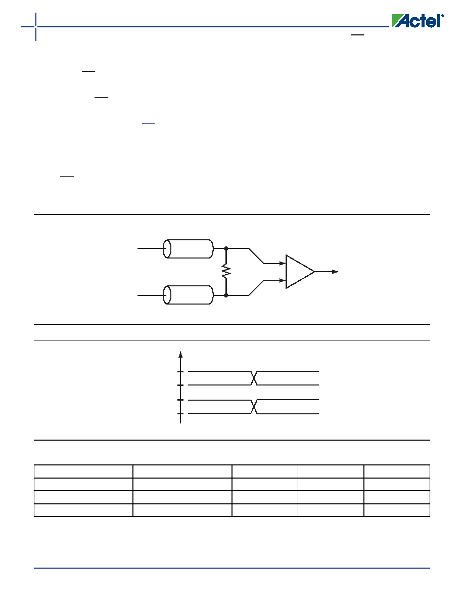
LVPECL Input Pads
In addition to standard I/O pads and power pads,
ProASICPLUS devices have a single LVPECL input pad on
both the east and west sides of the device, along with
AVDD and AGND pins to power the PLL block. The
LVPECL pad cell consists of an input buffer (containing a
low voltage differential amplifier) and a signal and its
complement, PPECL (I/P) (PECLN) and NPECL (PECLREF).
The LVPECL input pad cell differs from the standard I/O
cell in that it is operated from VDD only.
Since it is exclusively an input, it requires no output
signal, output enable signal, or output configuration
bits. As a special high-speed differential input, it also
does not require pull-ups. Recommended termination
for LVPECL inputs is shown in Figure 2-7. The LVPECL pad
cell compares voltages on the PPECL (I/P) pad (as
illustrated in Figure 2-8) and the NPECL pad and sends
the results to the global MUX (Figure 2-11 on page 2-11).
This high-speed, low-skew output essentially controls the
clock conditioning circuit.
LVPECLs are designed to meet LVPECL JEDEC receiver
standard levels (Table 2-5).
Figure 2-7 Recommended Termination for LVPECL Inputs
Figure 2-8 LVPECL High and Low Threshold Values
Table 2-5
LVPECL Receiver Specifications
Symbol
Parameter
Minimum
Maximum
Units
VIH
Input High Voltage
1.49
2.72
V
VIL
Input Low Voltage
0.86
2.125
V
VID
Differential Input Voltage
0.3
VDD
V
+
_
PPECL
NPECL
From LVPECL Driver
Data
Z = 50
Ω
0
Z = 50
Ω
0
R = 100
Ω
2.72
2.125
1.49
0.86
Voltage
相关PDF资料 |
PDF描述 |
|---|---|
| APA750-FGG676I | IC FPGA PROASIC+ 750K 676-FBGA |
| HSC43DRAS-S734 | CONN EDGECARD 86POS .100 R/A PCB |
| EP2SGX30DF780I4N | IC STRATIX II GX 30K 780-FBGA |
| 25AA160CT-I/MNY | IC SRL EEPROM 2KX8 1.8V 8-TDFN |
| ACC49DRXI-S734 | CONN EDGECARD 98POS DIP .100 SLD |
相关代理商/技术参数 |
参数描述 |
|---|---|
| APA750-FG896 | 功能描述:IC FPGA PROASIC+ 750K 896-FBGA RoHS:否 类别:集成电路 (IC) >> 嵌入式 - FPGA(现场可编程门阵列) 系列:ProASICPLUS 标准包装:1 系列:ProASICPLUS LAB/CLB数:- 逻辑元件/单元数:- RAM 位总计:129024 输入/输出数:248 门数:600000 电源电压:2.3 V ~ 2.7 V 安装类型:表面贴装 工作温度:- 封装/外壳:352-BFCQFP,带拉杆 供应商设备封装:352-CQFP(75x75) |
| APA750-FG896A | 功能描述:IC FPGA PROASIC+ 750K 896-FBGA RoHS:否 类别:集成电路 (IC) >> 嵌入式 - FPGA(现场可编程门阵列) 系列:ProASICPLUS 标准包装:1 系列:ProASICPLUS LAB/CLB数:- 逻辑元件/单元数:- RAM 位总计:129024 输入/输出数:248 门数:600000 电源电压:2.3 V ~ 2.7 V 安装类型:表面贴装 工作温度:- 封装/外壳:352-BFCQFP,带拉杆 供应商设备封装:352-CQFP(75x75) |
| APA750-FG896I | 功能描述:IC FPGA PROASIC+ 750K 896-FBGA RoHS:否 类别:集成电路 (IC) >> 嵌入式 - FPGA(现场可编程门阵列) 系列:ProASICPLUS 标准包装:1 系列:ProASICPLUS LAB/CLB数:- 逻辑元件/单元数:- RAM 位总计:129024 输入/输出数:248 门数:600000 电源电压:2.3 V ~ 2.7 V 安装类型:表面贴装 工作温度:- 封装/外壳:352-BFCQFP,带拉杆 供应商设备封装:352-CQFP(75x75) |
| APA750-FGB | 制造商:ACTEL 制造商全称:Actel Corporation 功能描述:ProASIC Flash Family FPGAs |
| APA750-FGES | 制造商:ACTEL 制造商全称:Actel Corporation 功能描述:ProASIC Flash Family FPGAs |
发布紧急采购,3分钟左右您将得到回复。