- 您现在的位置:买卖IC网 > PDF目录20503 > APEK4403GEU-01-T-DK (Allegro Microsystems Inc)BOARD EVAL FOR A4403 PDF资料下载
参数资料
| 型号: | APEK4403GEU-01-T-DK |
| 厂商: | Allegro Microsystems Inc |
| 文件页数: | 5/16页 |
| 文件大小: | 0K |
| 描述: | BOARD EVAL FOR A4403 |
| 标准包装: | 1 |
| 主要目的: | DC/DC,步降 |
| 输出及类型: | 1,非隔离 |
| 输入电压: | 9 V ~ 46 V |
| 稳压器拓扑结构: | 降压 |
| 板类型: | 完全填充 |
| 已供物品: | 板,CD |
| 已用 IC / 零件: | A4403 |
| 相关产品: | 620-1273-2-ND - IC REG BUCK ADJ 3A 16QFN |
| 其它名称: | 620-1387 |
�� �
�
�A4403�
�Valley� Current� Mode� Control� Buck� Converter�
�Functional� Description�
�?� V� OUT�
�–� 1� ?� ?� ,�
�?�
�?� V� FB�
�Basic Operation� TheA4403 is a buck converter that utilizes�
�valley� current-mode� control.� The� on-time� is� set� by� the� amount�
�of� current� that� flows� into� the� TON� pin.� This� is� determined� by� the�
�value� of� the� TON� resistors� chosen� (R1� and� R2� in� the� Functional�
�Block� diagram)� and� the� magnitude� of� the� input� voltage,� V� IN� .�
�Under� a� specific� set� of� conditions,� an� on-time� can� be� set� that�
�then� dictates� the� switching� frequency.� This� switching� frequency�
�remains� reasonably� constant� throughout� load� and� line� conditions�
�as� the� on-time� varies� inversely� with� the� input� voltage.� The� Switch�
�On-Time� and� Switching� Frequency� section� provides� more� details�
�on� this� subject.�
�At� the� beginning� of� the� switching� cycle,� the� buck� switch� is� turned�
�on� for� a� fixed� period� that� is� determined� by� the� current� flowing�
�into� TON.� Once� the� current� comparator� trips,� a� one-shot� mono-�
�stable,� the� On� Timer,� is� reset,� turning� off� the� switch.� The� current�
�through� the� inductor� then� decays.� This� current� is� sensed� through�
�the� external� sense� resistors� (R3� and� R4),� and� then� compared�
�against� the� current-demand� signal.� The� current-demand� signal� is�
�generated� by� comparing� the� output� voltage� against� an� accurate�
�bandgap� reference.� After� the� current� through� the� sense� resistors�
�decreases� to� the� valley� of� the� current-demand� signal,� the� On�
�Timer� is� set� to� turn� the� buck� switch� back� on� again� and� the� cycle� is�
�repeated.�
�Under� light� load� conditions,� the� converter� automatically� operates�
�in� pulse� frequency� modulation� (PFM)� mode� to� maintain� regu-�
�lation.� This� mode� of� operation� ensures� optimum� efficiency� as�
�switching� losses� are� reduced.�
�Overcurrent� Protection� The� converter� utilizes� pulse-by-pulse�
�valley� current� limiting,� which� operates� when� the� current� through�
�the� sense� resistors,� R3� and� R4� (set� for� 50� m� Ω� by� two� 100� m� Ω�
�resistors� in� parallel),� increases� above� 3.6� A� typical� at� the� valley�
�point.� The� corresponding� sense� voltage� (at� the� ISEN� pin)� that� cre-�
�ates� a� current� limiting� condition� is� 180� mV� typical.� It� is� possible,�
�by� careful� selection� of� the� sense� resistors,� to� reduce� the� current�
�limit� for� systems� with� maximum� loads� of� less� than� 3� A.�
�During� an� overload� condition,� the� switch� is� turned� on� for� the�
�period� determined� by� the� constant� on-time� circuitry.� The� switch�
�off-time� is� extended� until� the� current� decays� to� the� current� limit�
�value� of� 3.6� A� typical� (which� corresponds� to� a� sense� voltage� of�
�180� mV).� The� switch� is� then� turned� on� again.�
�Because� no� slope� compensation� is� required� in� this� control�
�scheme,� the� current� limit� is� maintained� at� a� reasonably� constant�
�level� across� the� input� voltage� range.�
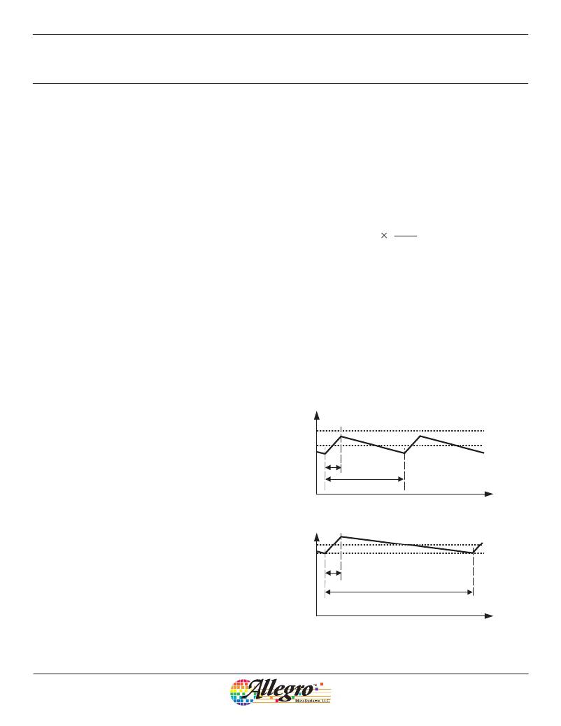
�Figure� 1� illustrates� how� the� current� is� limited� during� an� overload�
�condition.� The� current� decay� (period� with� switch� off)� is� propor-�
�tional� to� the� output� voltage.� As� the� overload� is� increased,� the� out-�
�put� voltage� tends� to� decrease� and� the� switching� period� increases.�
�Output� Voltage� Selection� The� output� voltage� of� the� converter�
�is� set� by� selecting� the� appropriate� feedback� resistors,� using� the�
�following� formula:�
�?�
�R� 5� =� R� 6� (1)�
�?� ?�
�where� (refering� to� the� Functional� Block� diagram):�
�R� 6� has� a� value� between� 750� Ω� and� 12� k� Ω� (R6� connected� between�
�the� GND� and� FB� pins),�
�R� 5� is� the� dependent� value� (R5� connected� between� the� output� rail�
�and� the� FB� pin),�
�V� OUT� is� the� user-configured� output� regulator� voltage,� and�
�V� FB� is� the� reference� voltage.�
�The� tolerance� of� the� feedback� resistors� influences� the� voltage� set-�
�point.� It� is� therefore� important� to� consider� the� tolerance� selection�
�when� targeting� an� overall� regulation� figure.�
�Inductor� current� operating� at� maximum� load�
�Current� Limit� level�
�Maximum� load�
�Constant� On-Time�
�Constant� period�
�Time�
�Inductor� current� operating� in� a� “soft”� overload�
�Overload�
�Current� Limit� level�
�Constant� On-Time�
�Extended� period�
�Time�
�Figure� 1.� Current� limiting� during� overload�
�Allegro� MicroSystems,� LLC�
�115� Northeast� Cutoff�
�Worcester,� Massachusetts� 01615-0036� U.S.A.�
�1.508.853.5000;� www.allegromicro.com�
�5�
�相关PDF资料 |
PDF描述 |
|---|---|
| AT88CK9000-TSU | CRYPTO PROGRAMMER BOARD 3-SOT23 |
| AT25080A-10TU-1.8 | IC EEPROM 8KBIT 20MHZ 8TSSOP |
| 8EWS12STRL | DIODE STD REC 1200V 8A D-PAK |
| AT25040AN-10SU-2.7 | IC EEPROM 4KBIT 20MHZ 8SOIC |
| 8EWS10STRL | DIODE STD REC 1000V 8A D-PAK |
相关代理商/技术参数 |
参数描述 |
|---|---|
| APEK4447SLJ-01-T-DK | 功能描述:A4447 - DC/DC, Step Down 1, Non-Isolated Outputs Evaluation Board 制造商:allegro microsystems, llc 系列:- 零件状态:有效 主要用途:DC/DC,步降 输出和类型:1,非隔离 功率 - 输出:- 电压 - 输出:0.8 V ~ 24 V 电流 - 输出:2A 电压 - 输入:8 V ~ 50 V 稳压器拓扑:降压 频率 - 开关:- 板类型:完全填充 所含物品:板 使用的 IC/零件:A4447 标准包装:1 |
| APEK4490EES-01-T-DK | 功能描述:BOARD EVAL FOR A4490 RoHS:是 类别:编程器,开发系统 >> 评估板 - DC/DC 与 AC/DC(离线)SMPS 系列:- 标准包装:1 系列:- 主要目的:DC/DC,步降 输出及类型:1,非隔离 功率 - 输出:- 输出电压:3.3V 电流 - 输出:3A 输入电压:4.5 V ~ 28 V 稳压器拓扑结构:降压 频率 - 开关:250kHz 板类型:完全填充 已供物品:板 已用 IC / 零件:L7981 其它名称:497-12113STEVAL-ISA094V1-ND |
| APEK4491EES-01-T-DK | 功能描述:A4491 - DC/DC, Step Down 3, Non-Isolated Outputs Evaluation Board 制造商:allegro microsystems, llc 系列:- 零件状态:有效 主要用途:DC/DC,步降 输出和类型:3,非隔离 功率 - 输出:- 电压 - 输出:- 电流 - 输出:- 电压 - 输入:4.5 V ~ 23 V 稳压器拓扑:降压 频率 - 开关:550kHz 板类型:完全填充 所含物品:板 使用的 IC/零件:A4491 标准包装:1 |
| APEK4900KLQ-01-T-DK | 功能描述:A4900 - Power Management, Half H-Bridge Driver (External FET) Evaluation Board 制造商:allegro microsystems, llc 系列:- 零件状态:过期 主要用途:电源管理,半 H 桥驱动器(外部 FET) 嵌入式:- 使用的 IC/零件:A4900 主要属性:3 个半 H 桥驱动器 辅助属性:- 所含物品:板 标准包装:1 |
| APEK4910KJP-01-T-DK | 功能描述:A4910 - Power Management, Half H-Bridge Driver (External FET) Evaluation Board 制造商:allegro microsystems, llc 系列:- 零件状态:有效 主要用途:电源管理,半 H 桥驱动器(外部 FET) 嵌入式:- 使用的 IC/零件:A4910 主要属性:3 个半 H 桥驱动器 辅助属性:- 所含物品:板 标准包装:1 |
发布紧急采购,3分钟左右您将得到回复。