- 您现在的位置:买卖IC网 > PDF目录166232 > AS7C25512NTD32A-166TQI (INTEGRATED SILICON SOLUTION INC) 512K X 32 ZBT SRAM, 3.5 ns, PQFP100 PDF资料下载
参数资料
| 型号: | AS7C25512NTD32A-166TQI |
| 厂商: | INTEGRATED SILICON SOLUTION INC |
| 元件分类: | SRAM |
| 英文描述: | 512K X 32 ZBT SRAM, 3.5 ns, PQFP100 |
| 封装: | 14 X 20 MM, TQFP-100 |
| 文件页数: | 15/18页 |
| 文件大小: | 428K |
| 代理商: | AS7C25512NTD32A-166TQI |
AS7C25512NTD32A/36A
12/23/04, v 2.2
Alliance Semiconductor
P. 6 of 18
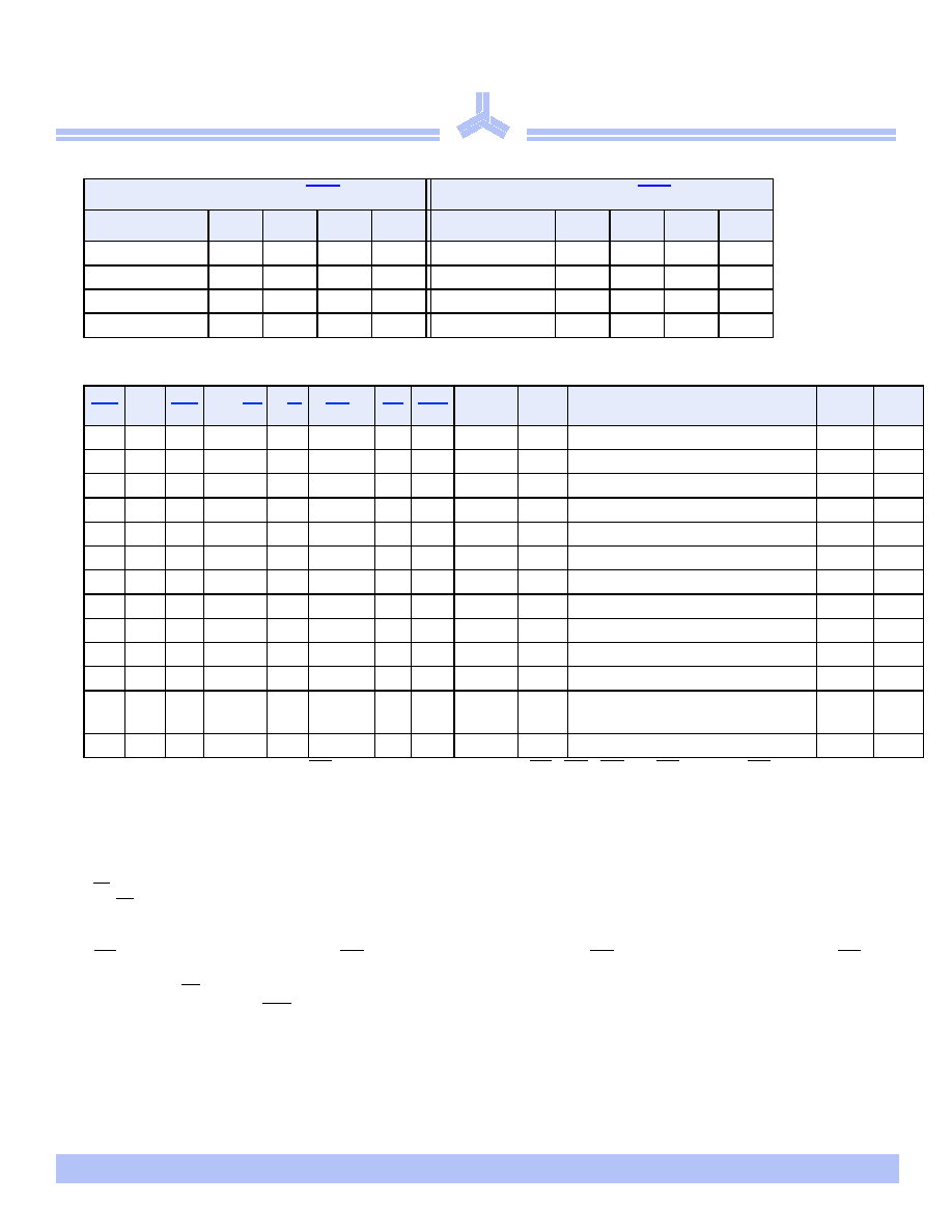
Burst order
Synchronous truth table[5,6,7,8,9,11]
Key: X = Don’t Care, H = HIGH, L = LOW.
BWn = H means all byte write signals (BWa, BWb, BWc, and BWd) are HIGH. BWn = L means one or
more byte write signals are LOW.
Notes:
1 CONTINUE BURST cycles, whether READ or WRITE, use the same control inputs. The type of cycle performed (READ or WRITE) is chose in the initial
BEGIN BURST cycle. A CONINUE DESELECT cycle can only be entered if a DESELECT CYCLE is executed first.
2 DUMMY READ and WRITE ABORT cycles can be considered NOPs because the device performs no external operation. A WRITE ABORT means a
WRITE command is given, but no operation is performed.
3 OE may be wired LOW to minimize the number of control signal to the SRAM. The device will automatically turn off the output drivers during a WRITE
cycle. OE may be used when the bus turn-on and turn-off times do not meet an application’s requirements.
4 If an INHIBIT CLOCK command occurs during a READ operation, the DQ bus will remain active (Low-Z). If it occurs during a WRITE cycle, the bus will
remain in High-Z. No WRITE operations will be performed during the INHIBIT CLOCK cycle.
5
BWa enables WRITEs to byte “a” (DQa pins); BWb enables WRITEs to byte “b” (DQb pins); BWc enables WRITEs to byte “c” (DQc pins); BWd
enables WRITEs to byte “d” (DQd pins).
6 All inputs except
OE and ZZ must meet setup and hold times around the rising edge (LOW to HIGH) of CLK.
7 Wait states are inserted by setting
CEN HIGH.
8 This device contains circuitry that will ensure that the outputs will be in High-Z during power-up.
9 The device incorporates a 2-bit burst counter. Address wraps to the initial address every fourth BURST CYCLE.
10 The address counter is incremented for all CONTINUE BURST cycles.
11 ZZ pin is always Low in this truth table.
Interleaved burst order (LBO = 1)
Linear burst order (LBO = 0)
A1 A0 A1 A0 A1 A0 A1 A0
Starting address
0 0
0 1
1 0
1 1
Starting Address
0 0
0 1
1 0
1 1
First increment
0 1
0 0
1 1
1 0
First increment
0 1
1 0
1 1
0 0
Second increment
1 0
1 1
0 0
0 1
Second increment
1 0
1 1
0 0
0 1
Third increment
1 1
1 0
0 1
0 0
Third increment
1 1
0 0
0 1
1 0
CE0 CE1 CE2 ADV/LD R/W
BWn
OE CEN
Address
source
CLK
Operation
DQ
Notes
H
X
L
X
L
NA
L to H
DESELECT Cycle
High-Z
X
H
L
X
L
NA
L to H
DESELECT Cycle
High-Z
X
L
X
L
X
L
NA
L to H
DESELECT Cycle
High-Z
X
H
X
L
NA
L to H
CONTINUE DESELECT Cycle
High-Z
1
L
H
L
H
X
L
External L to H
READ Cycle (Begin Burst)
Q
X
H
X
L
Next
L to H
READ Cycle (Continue Burst)
Q
1,10
L
H
L
H
X
H
L
External L to H NOP/DUMMY READ (Begin Burst) High-Z
2
X
H
X
H
L
Next
L to H
DUMMY READ (Continue Burst)
High-Z 1,2,10
L
H
L
X
L
External L to H
WRITE CYCLE (Begin Burst)
D
3
X
H
X
L
X
L
Next
L to H
WRITE CYCLE (Continue Burst)
D
1,3,10
L
H
L
H
X
L
External L to H NOP/WRITE ABORT (Begin Burst) High-Z
2,3
X
H
X
H
X
L
Next
L to H
WRITE ABORT (Continue Burst)
High-Z
1,2,3,
10
X
H
Current L to H
INHIBIT CLOCK
-
4
相关PDF资料 |
PDF描述 |
|---|---|
| AS7C3256K18Z-3.5TQC | 256K X 18 STANDARD SRAM, 3.5 ns, PQFP100 |
| AS7C33512NTD18A-166BC | 512K X 18 ZBT SRAM, 9 ns, PBGA119 |
| AS7C3364FT36B-65TQCN | 64K X 36 STANDARD SRAM, 6.5 ns, PQFP100 |
| AS7C3364FT36B-80TQC | 64K X 36 STANDARD SRAM, 8 ns, PQFP100 |
| AS7C34098-35JC | 256K X 16 STANDARD SRAM, 35 ns, PDSO44 |
相关代理商/技术参数 |
参数描述 |
|---|---|
| AS7C25512NTD32A-166TQIN | 制造商:ALSC 制造商全称:Alliance Semiconductor Corporation 功能描述:2.5V 512K x 32/36 Pipelined SRAM with NTD |
| AS7C25512NTD36A-133TQC | 制造商:ALSC 制造商全称:Alliance Semiconductor Corporation 功能描述:2.5V 512K x 32/36 Pipelined SRAM with NTD |
| AS7C25512NTD36A-133TQCN | 制造商:ALSC 制造商全称:Alliance Semiconductor Corporation 功能描述:2.5V 512K x 32/36 Pipelined SRAM with NTD |
| AS7C25512NTD36A-133TQI | 制造商:ALSC 制造商全称:Alliance Semiconductor Corporation 功能描述:2.5V 512K x 32/36 Pipelined SRAM with NTD |
| AS7C25512NTD36A-133TQIN | 制造商:ALSC 制造商全称:Alliance Semiconductor Corporation 功能描述:2.5V 512K x 32/36 Pipelined SRAM with NTD |
发布紧急采购,3分钟左右您将得到回复。