- 您现在的位置:买卖IC网 > PDF目录298831 > AS7C33512PFS16A-133BI (INTEGRATED SILICON SOLUTION INC) 512K X 16 STANDARD SRAM, 10 ns, PBGA119 PDF资料下载
参数资料
| 型号: | AS7C33512PFS16A-133BI |
| 厂商: | INTEGRATED SILICON SOLUTION INC |
| 元件分类: | SRAM |
| 英文描述: | 512K X 16 STANDARD SRAM, 10 ns, PBGA119 |
| 封装: | 14 X 20 MM, BGA-119 |
| 文件页数: | 10/14页 |
| 文件大小: | 370K |
| 代理商: | AS7C33512PFS16A-133BI |
AS7C33512PFS16A
AS7C33512PFS18A
4/15/02; v.1.5
Alliance Semiconductor
5 of 14
Note: Stresses greater than those listed under Absolute Maximum Ratings may cause permanent damage to the device. This is a stress rating only and functional opera-
tion of the device at these or any other conditions outside those indicated in the operational sections of this specification is not implied. Exposure to absolute
maximum rating conditions may affect reliability.
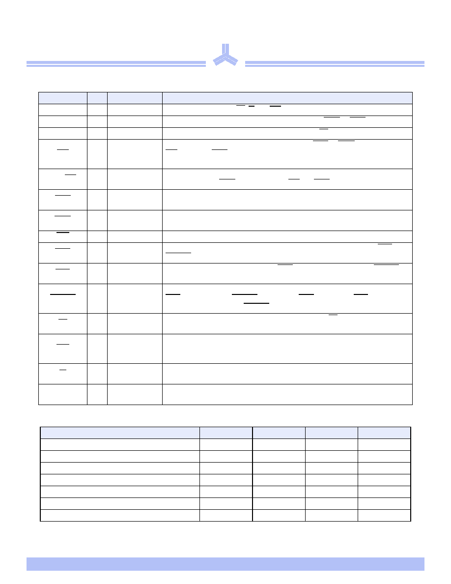
Signal descriptions
Signal
I/O
Properties
Description
CLK
I
CLOCK
Clock. All inputs except OE, FT, ZZ, LBO are synchronous to this clock.
A0–A18
I
SYNC
Address. Sampled when all chip enables are active and ADSC or ADSP are asserted.
DQ[a,b]
I/O
SYNC
Data. Driven as output when the chip is enabled and OE is active.
CE0
ISYNC
Master chip enable. Sampled on clock edges when ADSP or ADSC is active. When
CE0 is inactive, ADSP is blocked. Refer to the Synchronous Truth Table for more
information.
CE1, CE2
ISYNC
Synchronous chip enables. Active HIGH and active LOW, respectively. Sampled on
clock edges when ADSC is active or when CE0 and ADSP are active.
ADSP
ISYNC
Address strobe (processor). Asserted LOW to load a new address or to enter standby
mode.
ADSC
ISYNC
Address strobe (controller). Asserted LOW to load a new address or to enter standby
mode.
ADV
I
SYNC
Burst advance. Asserted LOW to continue burst read/write.
GWE
ISYNC
Global write enable. Asserted LOW to write all 16/18 bits. When HIGH, BWE and
BW[a,b] control write enable.
BWE
ISYNC
Byte write enable. Asserted LOW with GWE = HIGH to enable effect of BW[a,b]
inputs.
BW[a,b]
ISYNC
Write enables. Used to control write of individual bytes when GWE = HIGH and
BWE = LOW. If any of BW[a,b] is active with GWE = HIGH and BWE = LOW the
cycle is a write cycle. If all BW[a,b] are inactive, the cycle is a read cycle.
OE
IASYNC
Asynchronous output enable. I/O pins are driven when OE is active and the chip is
in read mode.
LBO
ISTATIC
Count mode. When driven HIGH, count sequence follows Intel XOR convention.
When driven LOW, count sequence follows linear convention. This signal is
internally pulled HIGH.
FT
ISTATIC
Flow-through mode.When LOW, enables single register flow-through mode.
Connect to VDD if unused or for pipelined operation.
ZZ
I
ASYNC
Snooze. Places device in low power mode; data is retained. Connect to GND if
unused.
Absolute maximum ratings
Parameter
Symbol
Min
Max
Unit
Power supply voltage relative to GND
VDD, VDDQ
–0.5
+4.6
V
Input voltage relative to GND (input pins)
VIN
–0.5
VDD + 0.5
V
Input voltage relative to GND (I/O pins)
VIN
–0.5
VDDQ + 0.5
V
Power dissipation
PD
–1.8
W
DC output current
IOUT
–50
mA
Storage temperature (plastic)
Tstg
–65
+150
°C
Temperature under bias
Tbias
–65
+135
°C
相关PDF资料 |
PDF描述 |
|---|---|
| AS7C33512PFS32A-225TQC | 512K X 32 STANDARD SRAM, 6.9 ns, PQFP100 |
| AS7C3364NTD36B-133TQIN | 64K X 36 ZBT SRAM, 4 ns, PQFP100 |
| AS7C3364NTD36B-200TQC | 64K X 36 ZBT SRAM, 3 ns, PQFP100 |
| ASD15-12D15 | 2-OUTPUT 7.5 W DC-DC REG PWR SUPPLY MODULE |
| ASD75-48S5Q-N | 1-OUTPUT 75 W DC-DC REG PWR SUPPLY MODULE |
相关代理商/技术参数 |
参数描述 |
|---|---|
| AS7C33512PFS18A | 制造商:ALSC 制造商全称:Alliance Semiconductor Corporation 功能描述:3.3V 512K x 18 pipeline burst synchronous SRAM |
| AS7C33512PFS18A-133TQC | 制造商:ALSC 制造商全称:Alliance Semiconductor Corporation 功能描述:3.3V 512K x 18 pipeline burst synchronous SRAM |
| AS7C33512PFS18A-133TQCN | 制造商:ALSC 制造商全称:Alliance Semiconductor Corporation 功能描述:3.3V 512K x 18 pipeline burst synchronous SRAM |
| AS7C33512PFS18A-133TQI | 制造商:ALSC 制造商全称:Alliance Semiconductor Corporation 功能描述:3.3V 512K x 18 pipeline burst synchronous SRAM |
| AS7C33512PFS18A-133TQIN | 制造商:ALSC 制造商全称:Alliance Semiconductor Corporation 功能描述:3.3V 512K x 18 pipeline burst synchronous SRAM |
发布紧急采购,3分钟左右您将得到回复。