- 您现在的位置:买卖IC网 > PDF目录11673 > AS8501-ASOU (ams)IC DATA ACQ 16-SOIC PDF资料下载
参数资料
| 型号: | AS8501-ASOU |
| 厂商: | ams |
| 文件页数: | 6/41页 |
| 文件大小: | 0K |
| 描述: | IC DATA ACQ 16-SOIC |
| 特色产品: | AS8501 High Precision Data Acquisition Ics |
| 标准包装: | 46 |
| 类型: | 数据采集系统(DAS) |
| 输入类型: | 模拟,数字 |
| 输出类型: | 模拟,数字 |
| 接口: | 串行 |
| 电流 - 电源: | 5mA |
| 安装类型: | 表面贴装 |
| 封装/外壳: | 16-SOIC(0.295",7.50mm 宽) |
| 供应商设备封装: | 16-SOIC |
| 包装: | 管件 |
| 产品目录页面: | 803 (CN2011-ZH PDF) |
第1页第2页第3页第4页第5页当前第6页第7页第8页第9页第10页第11页第12页第13页第14页第15页第16页第17页第18页第19页第20页第21页第22页第23页第24页第25页第26页第27页第28页第29页第30页第31页第32页第33页第34页第35页第36页第37页第38页第39页第40页第41页
AS8501 - Data Sheet
austriamicrosystems
Revision 1.1, 04-April-06
www.austriamicrosystems.com
Page 13 of 40
For an clock frequency of 8.192 MHz it can vary between
16 000 kHz and 1.95 Hz.
In the dual mode the ASSP is switching automatically between the two channels and it needs at least one measurement for each polarity to get a valid
measurement. In addition the ASSP needs some time to reprogram the internal registers and switches. Therefore the maximum sampling frequency is
limited to 7.5 kHz for the above given clock frequency. The internal averaging is not working in the dual mode, but the sampling frequency can be
different for each channel.
7.3.2
Calibration
The calibration of the ASSP is done by a test setup as follows:
-
room temperature calibration of the internal temperature sensor
-
absolute input-output calibration for all gain settings
-
TC calibration for the measurement path for gain 24
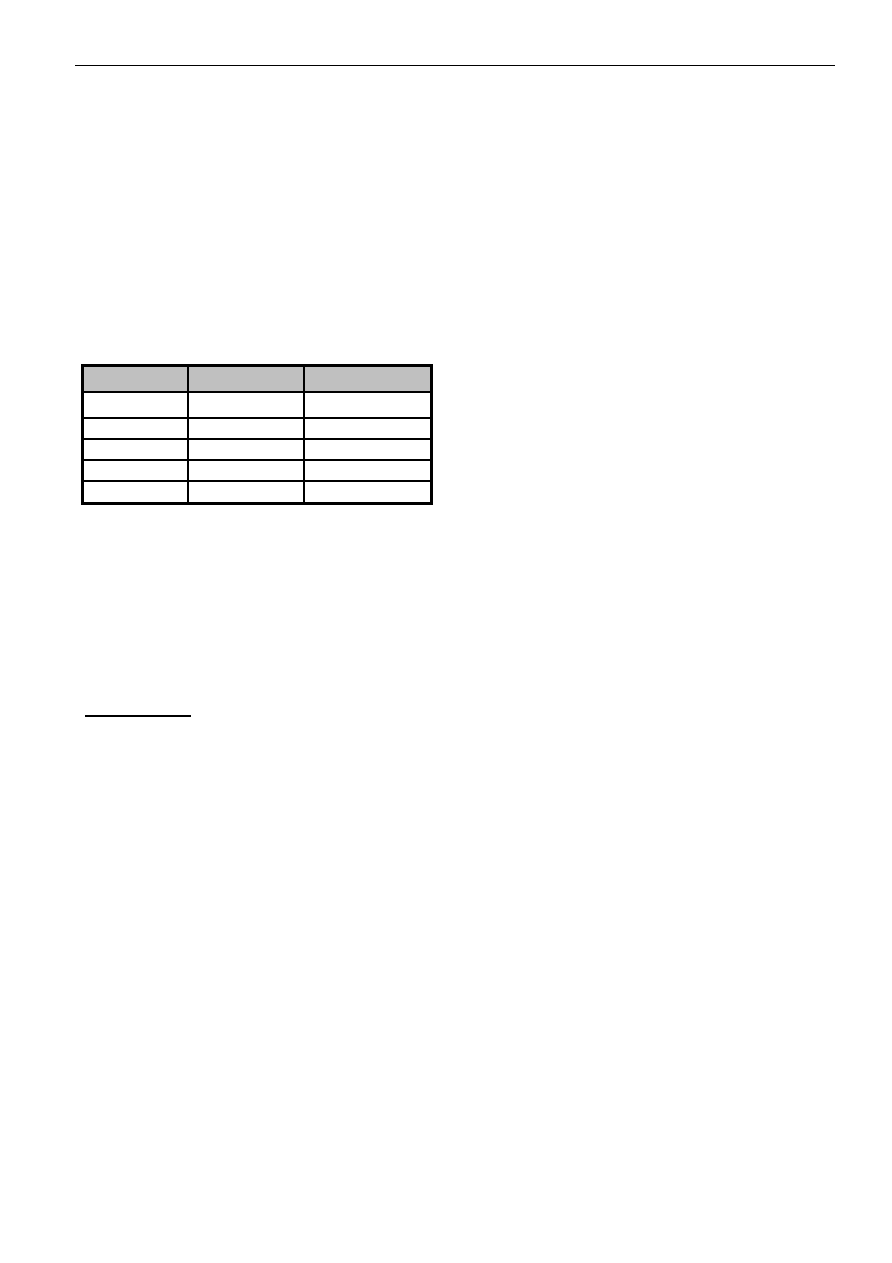
The absolute input-output calibration of the gain ranges is done that way that for a given input voltage 30 000 digits at the output are produced:
Table 7.2.2
In addition the ASSP receives an individual 24-bit serial number.
The TC-value of the output (total measurement path) for G24 is trimmed to a minimum value by selecting the best setting of the TRIMBTC subregister
of the TRR register (see 7.5.7).
A similar calibration is done for the other subregisters TRIMBV, TRIMA and TRIMC for the absolute value of the reference voltage, the offset of the PGA
and the current source respectively.
All these data are stored in the ZZR register according to the stored ZZR-register mapping‘ given in 8.6.2
7.4
Modes of operation
The AS8501 can run in different operation modes, which are selected and activated via the serial interface.
Detailed description:
Mode 0: MZL
In power-on reset sequence, which is initiated by the on-chip power-on reset circuit whenever the power is connected , the registers are loaded from the
Zener-Zap memory.
Mode 1: MMS
Measurement mode where the definition is taken from the registers CRA and CRG defined later on. The measurements are continuous and measured
results are available after the ready flag (INTN pin) is set to LO. The result can be read by the C any time after this bit is set to LO. However, to obtain
the best noise performances the result should be read when INTN pin is at LO state. All modules are in power-up.
Mode 2: MMD
Dual channel measurement mode. Two consecutive different measurements are performed according to the settings in the configuration registers CRA,
CRB and CRG defined later (usually CRA defining current measurements and CRB voltage measurement). One complete measurement is performed
with each setting. CRG register holds common settings.
The measurements are continuous (A,B,A,B). The 17th bit in the output register defines, which measurement has been executed according to the
definition LO=A, HI=B.
The number of consecutive measurements with equal configuration is defined in register CRG (bits s3,s2,s1,s0). All modules are in power-up.
Mode 3: MWU
In this wake-up mode the internal clock finclk=256kHz is running and one complete measurement is performed in the period from 1 to 1.5 s with the
parameter settings of the CRA register. Before the actual measurement is performed the logic powers up all internal circuits especially the AGND and
the Vref. If the external load is higher than 70 kOhms both signals can be used for external triggering or even as interrupt for the C.
If the external clock is not running, this input should be high impedance. To achieve a stable low idle current the oversampling ratio should be set to
R1=128 and the CFG register must be programmed to x00003, see also 7.5 ‘Register description’. It is assumed that the threshold level in the THR
register is defined within the 16 bit range, if not the default value is 210
After one measurement is finished all modules except the on- board oscillator and divider are switched into power down condition to save power. The
MSR register is updated with the last measurement result. Whenever this value exceeds the digital threshold the (wake-up) INTN pin goes LO for one
clock cycle to trigger the wake-up event in the external C.
gain
input/mV
output/digits
1
720
30 000
6
120
30 000
24
30
30 000
50
15
30 000
100
7.5
30 000
ams
AG
Technical
content
still
valid
相关PDF资料 |
PDF描述 |
|---|---|
| 227161-6 | CONN JACK BNC R/A 50OHM PCB AU |
| DF3048BF25WV | IC H8/3048 MCU FLASH 100QFP |
| R5F5630EDDFB#V0 | MCU RX630 2MB FLASH 144-LQFP |
| R5F56108VDFP#V0 | MCU 32BIT FLASH 2M ROM 144LQFP |
| MS27484E16F55S | CONN PLUG 55POS STRAIGHT W/SCKT |
相关代理商/技术参数 |
参数描述 |
|---|---|
| AS8501T&R | 制造商:AMSCO 制造商全称:austriamicrosystems AG 功能描述:High precision voltage and current measurement sensor interface |
| AS8501TR | 制造商:AMSCO 制造商全称:austriamicrosystems AG 功能描述:High precision voltage and current measurement sensor interface |
| AS8501TUB | 制造商:AMSCO 制造商全称:austriamicrosystems AG 功能描述:High precision voltage and current measurement sensor interface |
| AS85049-32-1 | 制造商:GLENAIR 制造商全称:Glenair, Inc. 功能描述:90° Adapter, Non-Environmental, RFI |
| AS8506 | 制造商:AMSCO 制造商全称:austriamicrosystems AG 功能描述:Battery Cell Monitor and Balancer IC |
发布紧急采购,3分钟左右您将得到回复。