- 您现在的位置:买卖IC网 > PDF目录42900 > AT-32032-BLK S BAND, Si, NPN, RF SMALL SIGNAL TRANSISTOR PDF资料下载
参数资料
| 型号: | AT-32032-BLK |
| 元件分类: | 小信号晶体管 |
| 英文描述: | S BAND, Si, NPN, RF SMALL SIGNAL TRANSISTOR |
| 封装: | ROHS COMPLIANT, MINIATURE, PLASTIC, SC-70, 3 PIN |
| 文件页数: | 3/14页 |
| 文件大小: | 1157K |
| 代理商: | AT-32032-BLK |
11
INPUT
Zo
C1
C4
C2
L2
R1
VCC = 3 V
R2
R4
C5
R5
L3
L4 C3
R6
Q1
L1
R3
OUTPUT
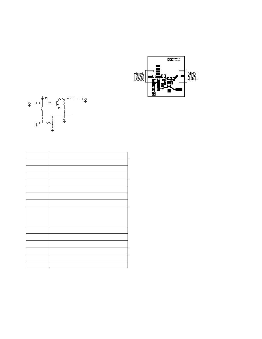
Figure 16. Schematic Diagram.
Figure 17. Component Parts List.
C1,C3
10 pF chip capacitor
C2
Open circuited stub .275 inch long
C4,C5
1000 pF chip capacitor
L1
8 nH chip inductor (Coilcraft 1008CS-080)
L2
Optional (see R1)
L3
56 nH chip inductor (Coilcraft 1008CS-560)
L4
15 nH chip inductor (Coilcraft 1008CS-150)
Q1 Silicon
Agilent AT-32032 Bipolar Transistor
R1
10 K
Ω chip resistor (may want to substitute
a 180 nH chip inductor and 50 W resistor for
lower noise figure, better low freq stability,
the readjust R2)
R2
26.1 K
Ω chip resistor (adjust for rated Ic)
R3
3.32 K
Ω chip resistor
R4
3.32 K
Ω chip resistor
R5
51.1
Ω chip resistor
R6
13
Ω chip resistor (see text)
Zo
50
Ω microstripline
AT-32032 Application Information
The AT-32032 is described in a low noise amplifier for use
in the 800 to 900 MHz frequency range. The amplifier is
designed for use with .032 inch thickness FR-4 printed
circuit board material.
900 MHz LNA Design
The amplifier is designed for a Vce of 2.7 volts and Ic of 5
mA. and a nominal power supply voltage of 3 volts. The
amplifier schematic is shown in Figure 16.
A component list is shown in Figure 17. The artwork
including component placement is shown in Figure 18.
Figure 18. 1X Artwork showing Component Placement.
The input matching network uses a shunt C series L input
impedance matching circuit for low noise. The shunt
C is accomplished with an open circuited stub while a
chip inductor is used for the series element. The output
impedance matching network consists of a series chip
inductor. Bias insertion is accomplished by the use of small
inductors suitably bypassed. A resistor is placed in series
with the output bias decoupling inductor to de-Q the
network and improve in-band and low frequency stability.
Surface mount Coilcraft inductors were chosen for their
small size. Resistor R6 enhances broad band stability
especially in the 9 to 10 GHz frequency range.
Biasing
The bias network is designed for a nominal power supply
voltage of 3 volts. Resistors R1 and R2 are used to adjust
collector current. Resistor R4 can be attached to the
junction of R5 and C5 to improve bias point stability.
IN
OUT
Vcc
AT-3XX32
AT-4XX32
02/98 AJW
.031 FR-4
相关PDF资料 |
PDF描述 |
|---|---|
| AT-32032-TR2G | S BAND, Si, NPN, RF SMALL SIGNAL TRANSISTOR |
| AT-32032-TR2 | S BAND, Si, NPN, RF SMALL SIGNAL TRANSISTOR |
| AT-32032-TR1 | S BAND, Si, NPN, RF SMALL SIGNAL TRANSISTOR |
| AT-32033-TR1 | S BAND, Si, NPN, RF SMALL SIGNAL TRANSISTOR |
| AT-32033-BLKG | S BAND, Si, NPN, RF SMALL SIGNAL TRANSISTOR |
相关代理商/技术参数 |
参数描述 |
|---|---|
| AT-32032-BLKG | 功能描述:射频双极小信号晶体管 Transistor Si Low Current RoHS:否 制造商:NXP Semiconductors 配置:Single 晶体管极性:NPN 最大工作频率:7000 MHz 集电极—发射极最大电压 VCEO:15 V 发射极 - 基极电压 VEBO:2 V 集电极连续电流:0.15 A 功率耗散:1000 mW 直流集电极/Base Gain hfe Min: 最大工作温度:+ 150 C 封装 / 箱体:SOT-223 封装:Reel |
| AT-32032-TR1 | 功能描述:IC TRANS NPN BIPOLAR SOT-323 RoHS:否 类别:分离式半导体产品 >> RF 晶体管 (BJT) 系列:- 产品变化通告:Product Discontinuation 17/Dec/2010 标准包装:1 系列:- 晶体管类型:NPN 电压 - 集电极发射极击穿(最大):4.7V 频率 - 转换:47GHz 噪声系数(dB典型值@频率):0.5dB ~ 1.45dB @ 150MHz ~ 10GHz 增益:9dB ~ 31dB 功率 - 最大:160mW 在某 Ic、Vce 时的最小直流电流增益 (hFE):160 @ 25mA,3V 电流 - 集电极 (Ic)(最大):45mA 安装类型:表面贴装 封装/外壳:4-SMD,扁平引线 供应商设备封装:4-TSFP 包装:Digi-Reel® 其它名称:BFP 740FESD E6327DKR |
| AT-32032-TR1G | 功能描述:射频双极小信号晶体管 Transistor Si Low Current RoHS:否 制造商:NXP Semiconductors 配置:Single 晶体管极性:NPN 最大工作频率:7000 MHz 集电极—发射极最大电压 VCEO:15 V 发射极 - 基极电压 VEBO:2 V 集电极连续电流:0.15 A 功率耗散:1000 mW 直流集电极/Base Gain hfe Min: 最大工作温度:+ 150 C 封装 / 箱体:SOT-223 封装:Reel |
| AT-32032-TR2 | 制造商:未知厂家 制造商全称:未知厂家 功能描述:TRANSISTOR | BJT | NPN | 5.5V V(BR)CEO | 40MA I(C) | SOT-323 |
| AT-32032-TR2G | 功能描述:射频双极小信号晶体管 Transistor Si Low Current RoHS:否 制造商:NXP Semiconductors 配置:Single 晶体管极性:NPN 最大工作频率:7000 MHz 集电极—发射极最大电压 VCEO:15 V 发射极 - 基极电压 VEBO:2 V 集电极连续电流:0.15 A 功率耗散:1000 mW 直流集电极/Base Gain hfe Min: 最大工作温度:+ 150 C 封装 / 箱体:SOT-223 封装:Reel |
发布紧急采购,3分钟左右您将得到回复。