- 您现在的位置:买卖IC网 > PDF目录20548 > AT45DB011B-CI (Atmel)IC FLASH 1MBIT 20MHZ 9CBGA PDF资料下载
参数资料
| 型号: | AT45DB011B-CI |
| 厂商: | Atmel |
| 文件页数: | 5/32页 |
| 文件大小: | 0K |
| 描述: | IC FLASH 1MBIT 20MHZ 9CBGA |
| 标准包装: | 490 |
| 格式 - 存储器: | 闪存 |
| 存储器类型: | DataFLASH |
| 存储容量: | 1M(512 页 x 264 字节) |
| 速度: | 20MHz |
| 接口: | SPI 3 线串行 |
| 电源电压: | 2.7 V ~ 3.6 V |
| 工作温度: | -40°C ~ 85°C |
| 封装/外壳: | 9-TBGA |
| 供应商设备封装: | 9-CBGA(5x5) |
| 包装: | 托盘 |
第1页第2页第3页第4页当前第5页第6页第7页第8页第9页第10页第11页第12页第13页第14页第15页第16页第17页第18页第19页第20页第21页第22页第23页第24页第25页第26页第27页第28页第29页第30页第31页第32页
�� �
�
�AT45DB011B�
�STATUS� REGISTER� READ:� The� status� register� can� be� used� to� determine� the� device� ’s�
�ready/busy� status,� the� result� of� a� Main� Memory� Page� to� Buffer� Compare� operation,� or� the�
�device� density.� To� read� the� status� register,� an� opcode� of� 57H� or� D7H� must� be� loaded� into� the�
�device.� After� the� last� bit� of� the� opcode� is� shifted� in,� the� eight� bits� of� the� status� register,� starting�
�with� the� MSB� (bit� 7),� will� be� shifted� out� on� the� SO� pin� during� the� next� eight� clock� cycles.� The�
�five� most� significant� bits� of� the� status� register� will� contain� device� information,� while� the� remain-�
�ing� three� least� significant� bits� are� reserved� for� future� use� and� will� have� undefined� values.� After�
�bit� 0� of� the� status� register� has� been� shifted� out,� the� sequence� will� repeat� itself� (as� long� as� CS�
�remains� low� and� SCK� is� being� toggled)� starting� again� with� bit� 7.� The� data� in� the� status� register�
�is� constantly� updated,� so� each� repeating� sequence� will� output� new� data.�
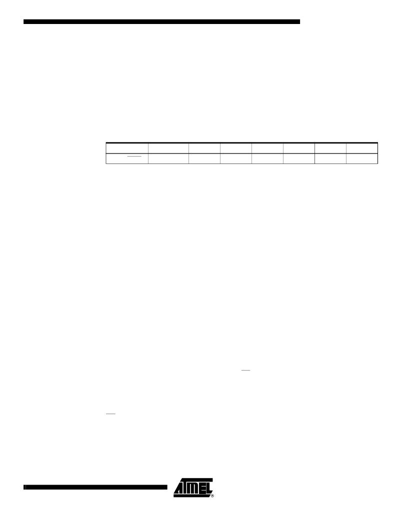
�Status� Register� Format�
�Bit� 7�
�RDY/BUSY�
�Bit� 6�
�COMP�
�Bit� 5�
�0�
�Bit� 4�
�0�
�Bit� 3�
�1�
�Bit� 2�
�1�
�Bit� 1�
�X�
�Bit� 0�
�X�
�Ready/Busy� status� is� indicated� using� bit� 7� of� the� status� register.� If� bit� 7� is� a� 1,� then� the� device�
�is� not� busy� and� is� ready� to� accept� the� next� command.� If� bit� 7� is� a� 0,� then� the� device� is� in� a� busy�
�state.� The� user� can� continuously� poll� bit� 7� of� the� status� register� by� stopping� SCK� at� a� low� level�
�once� bit� 7� has� been� output.� The� status� of� bit� 7� will� continue� to� be� output� on� the� SO� pin,� and�
�once� the� device� is� no� longer� busy,� the� state� of� SO� will� change� from� 0� to� 1.� There� are� eight�
�operations� which� can� cause� the� device� to� be� in� a� busy� state:� Main� Memory� Page� to� Buffer�
�Transfer,� Main� Memory� Page� to� Buffer� Compare,� Buffer� to� Main� Memory� Page� Program� with�
�Built-in� Erase,� Buffer� to� Main� Memory� Page� Program� without� Built-in� Erase,� Page� Erase,�
�Block� Erase,� Main� Memory� Page� Program,� and� Auto� Page� Rewrite.�
�The� result� of� the� most� recent� Main� Memory� Page� to� Buffer� Compare� operation� is� indicated�
�using� bit� 6� of� the� status� register.� If� bit� 6� is� a� 0,� then� the� data� in� the� main� memory� page� matches�
�the� data� in� the� buffer.� If� bit� 6� is� a� 1,� then� at� least� one� bit� of� the� data� in� the� main� memory� page�
�does� not� match� the� data� in� the� buffer.�
�The� device� density� is� indicated� using� bits� 5,� 4,� 3� and� 2� of� the� status� register.� For� the�
�AT45DB011B,� the� four� bits� are� 0,� 0,� 1� and� 1.� The� decimal� value� of� these� four� binary� bits� does�
�not� equate� to� the� device� density;� the� three� bits� represent� a� combinational� code� relating� to� dif-�
�fering� densities� of� Serial� DataFlash� devices,� allowing� a� total� of� sixteen� different� density�
�configurations.�
�Program� and�
�Erase� Commands�
�BUFFER� WRITE:� Data� can� be� shifted� in� from� the� SI� pin� into� the� data� buffer.� To� load� data� into�
�the� buffer,� an� 8-bit� opcode� of� 84H� is� followed� by� 15� don’t� care� bits� and� nine� address� bits�
�(BFA8-BFA0).� The� nine� address� bits� specify� the� first� byte� in� the� buffer� to� be� written.� The� data�
�is� entered� following� the� address� bits.� If� the� end� of� the� data� buffer� is� reached,� the� device� will�
�wrap� around� back� to� the� beginning� of� the� buffer.� Data� will� continue� to� be� loaded� into� the� buffer�
�until� a� low-to-high� transition� is� detected� on� the� CS� pin.�
�BUFFER� TO� MAIN� MEMORY� PAGE� PROGRAM� WITH� BUILT-IN� ERASE:� Data� written� into�
�the� buffer� can� be� programmed� into� the� main� memory.� An� 8-bit� opcode� of� 83H� is� followed� by�
�the� six� reserved� bits,� nine� address� bits� (PA8-PA0)� that� specify� the� page� in� the� main� memory�
�to� be� written,� and� nine� additional� don’t� care� bits.� When� a� low-to-high� transition� occurs� on� the�
�CS� pin,� the� part� will� first� erase� the� selected� page� in� main� memory� to� all� 1s� and� then� program�
�the� data� stored� in� the� buffer� into� the� specified� page� in� the� main� memory.� Both� the� erase� and�
�the� programming� of� the� page� are� internally� self-timed� and� should� take� place� in� a� maximum�
�time� of� t� EP� .� During� this� time,� the� status� register� will� indicate� that� the� part� is� busy.�
�5�
�1984J–DFLASH–06/06�
�相关PDF资料 |
PDF描述 |
|---|---|
| A7SXB-5006M | CABLE D-SUB - AFM50B/AE50M/X |
| AT45DB011B-CC | IC FLASH 1MBIT 20MHZ 9CBGA |
| T525T336M008ATE080 | CAP TANT 33UF 8V 20% 1411 |
| VI-B3P-CY-B1 | CONVERTER MOD DC/DC 13.8V 50W |
| BAT54SW-7 | DIODE SCHOTTKY 30V 200MW SC70-3 |
相关代理商/技术参数 |
参数描述 |
|---|---|
| AT45DB011B-SC | 功能描述:闪存 1M SERIAL 2.7V - COM TEMP RoHS:否 制造商:ON Semiconductor 数据总线宽度:1 bit 存储类型:Flash 存储容量:2 MB 结构:256 K x 8 定时类型: 接口类型:SPI 访问时间: 电源电压-最大:3.6 V 电源电压-最小:2.3 V 最大工作电流:15 mA 工作温度:- 40 C to + 85 C 安装风格:SMD/SMT 封装 / 箱体: 封装:Reel |
| AT45DB011B-SI | 功能描述:闪存 1M SERIAL 2.7V - IND TEMP RoHS:否 制造商:ON Semiconductor 数据总线宽度:1 bit 存储类型:Flash 存储容量:2 MB 结构:256 K x 8 定时类型: 接口类型:SPI 访问时间: 电源电压-最大:3.6 V 电源电压-最小:2.3 V 最大工作电流:15 mA 工作温度:- 40 C to + 85 C 安装风格:SMD/SMT 封装 / 箱体: 封装:Reel |
| AT45DB011B-SU | 功能描述:闪存 1M 8 I/O SPI 264B 2.7V RoHS:否 制造商:ON Semiconductor 数据总线宽度:1 bit 存储类型:Flash 存储容量:2 MB 结构:256 K x 8 定时类型: 接口类型:SPI 访问时间: 电源电压-最大:3.6 V 电源电压-最小:2.3 V 最大工作电流:15 mA 工作温度:- 40 C to + 85 C 安装风格:SMD/SMT 封装 / 箱体: 封装:Reel |
| AT45DB011B-XC | 功能描述:闪存 1M SERIAL 2.7V - COM TEMP RoHS:否 制造商:ON Semiconductor 数据总线宽度:1 bit 存储类型:Flash 存储容量:2 MB 结构:256 K x 8 定时类型: 接口类型:SPI 访问时间: 电源电压-最大:3.6 V 电源电压-最小:2.3 V 最大工作电流:15 mA 工作温度:- 40 C to + 85 C 安装风格:SMD/SMT 封装 / 箱体: 封装:Reel |
| AT45DB011B-XI | 功能描述:闪存 DATAFLASH 1M SERIAL 2.7V TSSOP IND TEMP RoHS:否 制造商:ON Semiconductor 数据总线宽度:1 bit 存储类型:Flash 存储容量:2 MB 结构:256 K x 8 定时类型: 接口类型:SPI 访问时间: 电源电压-最大:3.6 V 电源电压-最小:2.3 V 最大工作电流:15 mA 工作温度:- 40 C to + 85 C 安装风格:SMD/SMT 封装 / 箱体: 封装:Reel |
发布紧急采购,3分钟左右您将得到回复。