- 您现在的位置:买卖IC网 > PDF目录381453 > AT45DB021B-TU (ATMEL CORP) 2-megabit 2.7-volt Only DataFlash PDF资料下载
参数资料
| 型号: | AT45DB021B-TU |
| 厂商: | ATMEL CORP |
| 元件分类: | DRAM |
| 英文描述: | 2-megabit 2.7-volt Only DataFlash |
| 中文描述: | 2M X 1 FLASH 2.7V PROM, PDSO28 |
| 封装: | 18 X 13.40 MM, GREEN, PLASTIC, MO-183, TSOP1-28 |
| 文件页数: | 7/32页 |
| 文件大小: | 304K |
| 代理商: | AT45DB021B-TU |
第1页第2页第3页第4页第5页第6页当前第7页第8页第9页第10页第11页第12页第13页第14页第15页第16页第17页第18页第19页第20页第21页第22页第23页第24页第25页第26页第27页第28页第29页第30页第31页第32页
7
1937J–DFLSH–9/05
AT45DB021B
5.2.4
Page Erase
The optional Page Erase command can be used to individually erase any page in the main
memory array allowing the Buffer to Main Memory Page Program without Built-in Erase com-
mand to be utilized at a later time. To perform a Page Erase, an opcode of 81H must be loaded
into the device, followed by five reserved bits, ten address bits (PA9-PA0), and nine don’t care
bits. The ten address bits are used to specify which page of the memory array is to be erased.
When a low-to-high transition occurs on the CS pin, the part will erase the selected page to 1s.
The erase operation is internally self-timed and should take place in a maximum time of t
PE
. Dur-
ing this time, the status register will indicate that the part is busy.
5.2.5
Block Erase
A block of eight pages can be erased at one time allowing the Buffer to Main Memory Page Pro-
gram without Built-in Erase command to be utilized to reduce programming times when writing
large amounts of data to the device. To perform a Block Erase, an opcode of 50H must be
loaded into the device, followed by five reserved bits, seven address bits (PA9-PA3), and 12
don’t care bits. The seven address bits are used to specify which block of eight pages is to be
erased. When a low-to-high transition occurs on the CS pin, the part will erase the selected
block of eight pages to 1s. The erase operation is internally self-timed and should take place in a
maximum time of t
BE
. During this time, the status register will indicate that the part is busy.
5.2.6
Main Memory Page Program through Buffer
This operation is a combination of the Buffer Write and Buffer to Main Memory Page Program
with Built-in Erase operations. Data is first shifted into buffer 1 or buffer 2 from the SI pin and
then programmed into a specified page in the main memory. To initiate the operation, an 8-bit
opcode (82H for buffer 1 or 85H for buffer 2) must be followed by the five reserved bits and 20
address bits. The 10 most-significant address bits (PA9-PA0) select the page in the main mem-
ory where data is to be written, and the next nine address bits (BFA8-BFA0) select the first byte
in the buffer to be written. After all address bits are shifted in, the part will take data from the SI
pin and store it in one of the data buffers. If the end of the buffer is reached, the device will wrap
around back to the beginning of the buffer. When there is a low-to-high transition on the CS pin,
the part will first erase the selected page in main memory to all 1s and then program the data
stored in the buffer into the specified page in the main memory. Both the erase and the program-
ming of the page are internally self-timed and should take place in a maximum of time t
EP
.
During this time, the status register will indicate that the part is busy.
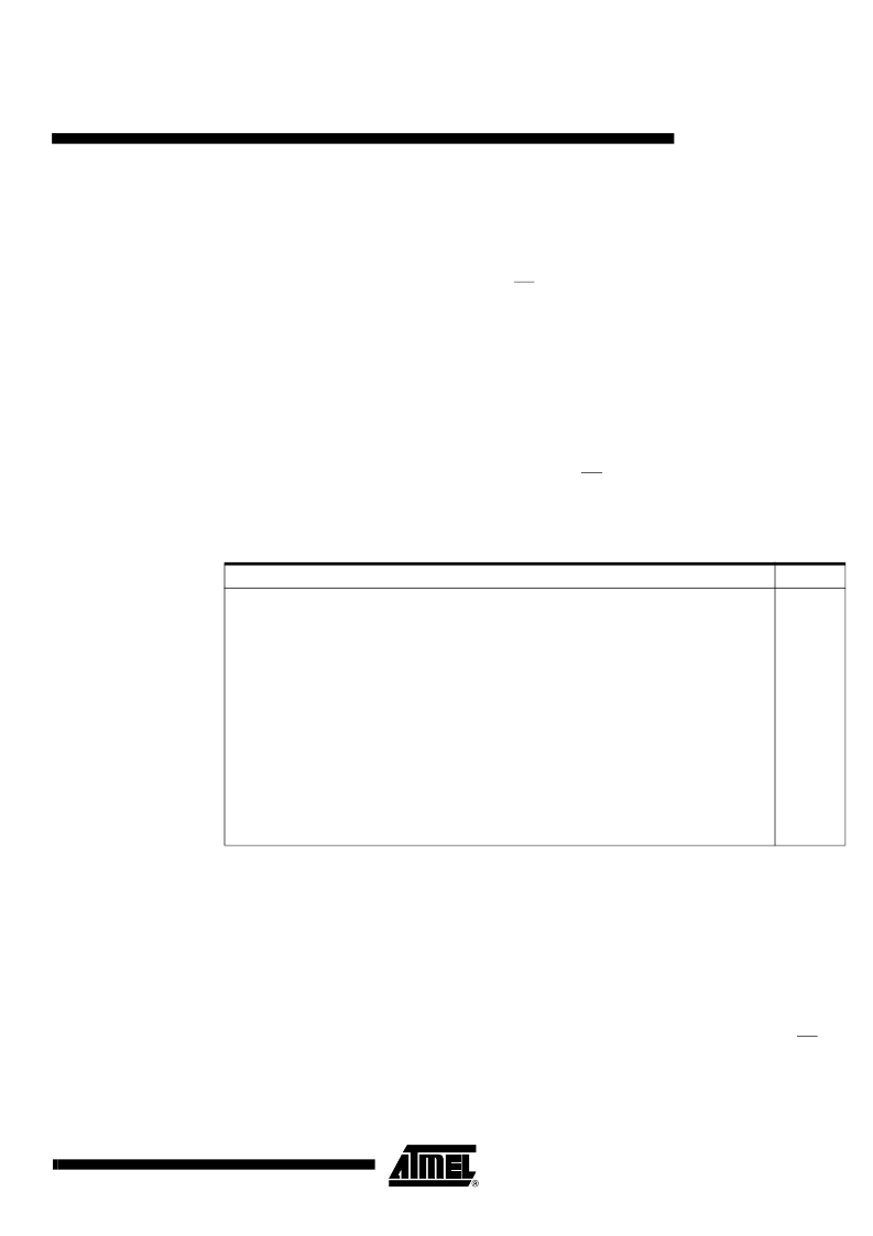
Table 5-2.
Block Erase Addressing
PA9
PA8
PA7
PA6
PA5
PA4
PA3
PA2
PA1
PA0
Block
0
0
0
0
0
0
0
X
X
X
0
0
0
0
0
0
0
1
X
X
X
1
0
0
0
0
0
1
0
X
X
X
2
0
0
0
0
0
1
1
X
X
X
3
1
1
1
1
1
0
0
X
X
X
124
1
1
1
1
1
0
1
X
X
X
125
1
1
1
1
1
1
0
X
X
X
126
1
1
1
1
1
1
1
X
X
X
127
相关PDF资料 |
PDF描述 |
|---|---|
| AT45DB021B-SC | 2-megabit 2.7-volt Only DataFlash?? |
| AT45DB021B-CC | 2-megabit 2.7-volt Only DataFlash?? |
| AT45DB021B-CI | 2-megabit 2.7-volt Only DataFlash?? |
| AT45DB021B-RC | 2-megabit 2.7-volt Only DataFlash?? |
| AT45DB021B-RI | 2-megabit 2.7-volt Only DataFlash?? |
相关代理商/技术参数 |
参数描述 |
|---|---|
| AT45DB021D | 制造商:ATMEL 制造商全称:ATMEL Corporation 功能描述:2-megabit 2.7-volt DataFlash |
| AT45DB021D_07 | 制造商:ATMEL 制造商全称:ATMEL Corporation 功能描述:2-megabit 2.7-volt DataFlash |
| AT45DB021D_08 | 制造商:ATMEL 制造商全称:ATMEL Corporation 功能描述:2-megabit 2.7-volt Minimum DataFlash |
| AT45DB021D_09 | 制造商:ATMEL 制造商全称:ATMEL Corporation 功能描述:2-megabit 2.7-volt Minimum DataFlash |
| AT45DB021D-MH-SL954 | 制造商:Adesto Technologies Corporation 功能描述:8-UDFN (5X6), IND TEMP, 2.7V, TRAY, 256 BYTE PAGE - Trays |
发布紧急采购,3分钟左右您将得到回复。