- 您现在的位置:买卖IC网 > PDF目录381460 > AT49LV040 (Atmel Corp.) 512K x 8 Single 2.7-volt Battery-Voltage Flash Memory(512K x 8单电源2.7V Battery-Voltage技术闪速存储器) PDF资料下载
参数资料
| 型号: | AT49LV040 |
| 厂商: | Atmel Corp. |
| 英文描述: | 512K x 8 Single 2.7-volt Battery-Voltage Flash Memory(512K x 8单电源2.7V Battery-Voltage技术闪速存储器) |
| 中文描述: | 为512k × 8单2.7伏电池电压快闪记忆体(为512k × 8单电源为2.7V电池电压技术闪速存储器) |
| 文件页数: | 2/14页 |
| 文件大小: | 278K |
| 代理商: | AT49LV040 |
AT49BV/LV040(T)
2
To allow for simple in-system reprogrammability, the
AT49BV/LV040(T) does not require high input voltages for
programming. Three-volt-only commands determine the
read and programming operation of the device. Reading
data out of the device is similar to reading from an EPROM.
Reprogramming the AT49BV/LV040(T) is performed by
erasing the entire four megabits of memory and then pro-
gramming on a byte-by-byte basis. The typical byte
programming time is a fast 30 μs. The end of a program
cycle can be optionally detected by the Data Polling
feature. Once the end of a byte program cycle has been
detected, a new access for a read or program can begin.
The typical number of program and erase cycles is in
excess of 10,000 cycles.
The optional 16K bytes boot block section includes a repro-
gramming write lockout feature to provide data integrity.
The boot sector is designed to contain user-secure code,
and when the feature is enabled, the boot sector is perma-
nently protected from being reprogrammed.
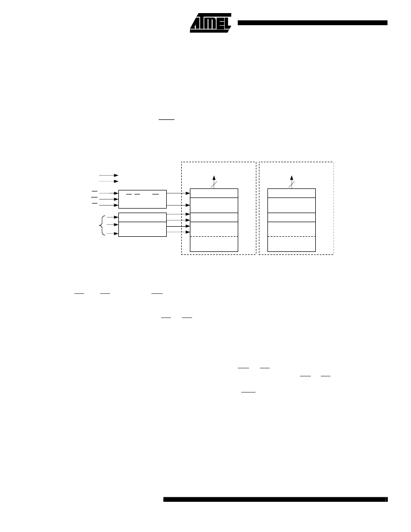
Block Diagram
Device Operation
READ:
The AT49BV/LV040(T) is accessed like an
EPROM. When CE and OE are low and WE is high, the
data stored at the memory location determined by the
address pins is asserted on the outputs. The outputs are
put in the high-impedance state whenever CE or OE is
high. This dual-line control gives designers flexibility in pre-
venting bus contention.
ERASURE:
Before a byte can be reprogrammed, the 512K
bytes memory array (or 496K bytes if the boot block fea-
tured is used) must be erased. The erased state of the
memory bits is a logical
“
1
”
. The entire device can be
erased at one time by using a six-byte software code. The
software chip erase code consists of six-byte load com-
mands to specific address locations with a specific data
pattern (please refer to
“
Chip Erase Cycle Waveforms
”
on
page 8).
After the software chip erase has been initiated, the device
will internally time the erase operation so that no external
clocks are required. The maximum time needed to erase
the whole chip is t
EC
. If the boot block lockout feature has
been enabled, the data in the boot sector will not be
erased.
BYTE PROGRAMMING:
Once the memory array is
erased, the device is programmed (to a logical
“
0
”
) on a
byte-by-byte basis. Please note that a data
“
0
”
cannot be
programmed back to a
“
1
”
; only erase operations can con-
vert
“
0
”
s to
“
1
”
s. Programming is accomplished via the
internal device command register and is a four-bus cycle
operation (please refer to the Command Definitions table).
The device will automatically generate the required internal
program pulses.
The program cycle has addresses latched on the falling
edge of WE or CE, whichever occurs last, and the data
latched on the rising edge of WE or CE, whichever occurs
first. Programming is completed after the specified t
BP
cycle
time. The Data Polling feature may also be used to indicate
the end of a program cycle.
BOOT BLOCK PROGRAMMING LOCKOUT:
The device
has one designated block that has a programming lockout
feature. This feature prevents programming of data in the
designated block once the feature has been enabled. The
size of the block is 16K bytes. This block, referred to as the
boot block, can contain secure code that is used to bring up
the system. Enabling the lockout feature will allow the boot
OE, CE, AND WE
LOGIC
Y DECODER
X DECODER
INPUT/OUTPUT
BUFFERS
DATA LATCH
Y-GATING
OPTIONAL BOOT
BLOCK (16K BYTES)
MAIN MEMORY
(496K BYTES)
OE
WE
CE
ADDRESS
INPUTS
VCC
GND
DATA INPUTS/OUTPUTS
I/O7 - I/O0
8
04000H
03FFFH
00000H
INPUT/OUTPUT
BUFFERS
DATA LATCH
Y-GATING
OPTIONAL BOOT
BLOCK (16K BYTES)
MAIN MEMORY
(496K BYTES)
7C000H
7BFFFH
00000H
AT49BV/LV040T
AT49BV/LV040
DATA INPUTS/OUTPUTS
I/O7 - I/O0
8
7FFFFH
7FFFFH
相关PDF资料 |
PDF描述 |
|---|---|
| AT49BV080 | 8-Megabit Single 2.7-volt Battery-Voltage Flash Memory(8M位单电源2.7V Battery-Voltage技术闪速存储器) |
| AT49LV080 | 8-Megabit Single 2.7-volt Battery-Voltage Flash Memory(8M位单电源2.7V Battery-Voltage技术闪速存储器) |
| AT49LV080T | 8-Megabit Single 2.7-volt Battery-Voltage Flash Memory(8M位单电源2.7V Battery-Voltage技术闪速存储器) |
| AT49BV1024A | 1-megabit (64K x 16) 3-volt Only Flash Memory |
| AT49LV1024A | 1-megabit (64K x 16) 3-volt Only Flash Memory |
相关代理商/技术参数 |
参数描述 |
|---|---|
| AT49LV040-12JC | 功能描述:闪存 4M bit RoHS:否 制造商:ON Semiconductor 数据总线宽度:1 bit 存储类型:Flash 存储容量:2 MB 结构:256 K x 8 定时类型: 接口类型:SPI 访问时间: 电源电压-最大:3.6 V 电源电压-最小:2.3 V 最大工作电流:15 mA 工作温度:- 40 C to + 85 C 安装风格:SMD/SMT 封装 / 箱体: 封装:Reel |
| AT49LV040-12JI | 功能描述:闪存 4M bit RoHS:否 制造商:ON Semiconductor 数据总线宽度:1 bit 存储类型:Flash 存储容量:2 MB 结构:256 K x 8 定时类型: 接口类型:SPI 访问时间: 电源电压-最大:3.6 V 电源电压-最小:2.3 V 最大工作电流:15 mA 工作温度:- 40 C to + 85 C 安装风格:SMD/SMT 封装 / 箱体: 封装:Reel |
| AT49LV040-12TC | 功能描述:闪存 4M bit RoHS:否 制造商:ON Semiconductor 数据总线宽度:1 bit 存储类型:Flash 存储容量:2 MB 结构:256 K x 8 定时类型: 接口类型:SPI 访问时间: 电源电压-最大:3.6 V 电源电压-最小:2.3 V 最大工作电流:15 mA 工作温度:- 40 C to + 85 C 安装风格:SMD/SMT 封装 / 箱体: 封装:Reel |
| AT49LV040-12TI | 功能描述:IC FLASH 4MBIT 120NS 32TSOP RoHS:否 类别:集成电路 (IC) >> 存储器 系列:- 标准包装:378 系列:- 格式 - 存储器:闪存 存储器类型:FLASH 存储容量:8M(1M x 8,512K x 16) 速度:110ns 接口:并联 电源电压:2.7 V ~ 3.6 V 工作温度:-40°C ~ 85°C 封装/外壳:48-CBGA 供应商设备封装:48-CBGA(7x7) 包装:托盘 |
| AT49LV040-12VC | 功能描述:闪存 4M bit RoHS:否 制造商:ON Semiconductor 数据总线宽度:1 bit 存储类型:Flash 存储容量:2 MB 结构:256 K x 8 定时类型: 接口类型:SPI 访问时间: 电源电压-最大:3.6 V 电源电压-最小:2.3 V 最大工作电流:15 mA 工作温度:- 40 C to + 85 C 安装风格:SMD/SMT 封装 / 箱体: 封装:Reel |
发布紧急采购,3分钟左右您将得到回复。