- 您现在的位置:买卖IC网 > PDF目录381463 > AT49LV8011 (Atmel Corp.) 8-megabit 3-volt Flash Memory(8M位 3V闪速存储器) PDF资料下载
参数资料
| 型号: | AT49LV8011 |
| 厂商: | Atmel Corp. |
| 英文描述: | 8-megabit 3-volt Flash Memory(8M位 3V闪速存储器) |
| 中文描述: | 8兆位3伏的快闪记忆体(800万位3V的闪速存储器) |
| 文件页数: | 2/18页 |
| 文件大小: | 322K |
| 代理商: | AT49LV8011 |
AT49BV/LV8011(T)
2
contention. This device can be read or reprogrammed
using a single 2.7V power supply, making it ideally suited
for in-system programming.
The device powers on in the read mode. Command
sequences are used to place the device in other operation
modes such as Program and Erase. The device has the
capability to protect the data in any sector. Once the data
protection for a given sector is enabled, the data in that
sector cannot be changed using input levels between
ground and V
CC
.
The device is segmented into two memory planes. Reads
from memory plane B may be performed even while pro-
gram or erase functions are being executed in memory
plane A and vice versa. This operation allows improved
system performance by not requiring the system to wait for
a program or erase operation to complete before a read is
performed. To further increase the flexibility of the device, it
contains an Erase Suspend feature. This feature will put
the Erase on hold for any amount of time and let the user
read data from or program data to any of the remaining
sectors within the same memory plane. There is no reason
to suspend the erase operation if the data to be read is in
the other memory plane. The end of a program or an Erase
cycle is detected by the Ready/Busy pin, Data polling, or by
the toggle bit.
A VPP pin is provided to improve program/erase times.
This pin can be tied to V
CC
. To take advantage of faster
programming and erasing, the pin should supply 4.5 to
5.5 volts during program and erase operations.
A 6-byte command (bypass unlock) sequence to remove
the requirement of entering the 3-byte program sequence
is offered to further improve programming time. After enter-
ing the 6-byte code, only single pulses on the write control
lines are required for writing into the device. This mode
(single-pulse byte/word program) is exited by powering
down the device, or by pulsing the RESET pin low for a
minimum of 50 ns and then bringing it back to V
CC
. Erase
and Erase Suspend/Resume commands will not work while
in this mode; if entered they will result in data being pro-
grammed into the device. It is not recommended that the
6-byte code reside in the software of the final product but
only exist in external programming code.
The BYTE pin controls whether the device data I/O pins
operate in the byte or word configuration. If the BYTE pin is
set at logic
“
1
”
, the device is in word configuration,
I/O0 - I/O15 are active and controlled by CE and OE.
If the BYTE pin is set at logic
“
0
”
, the device is in byte con-
figuration, and only data I/O pins I/O0 - I/O7 are active and
controlled by CE and OE. The data I/O pins I/O8 - I/O14
are tri-stated, and the I/O15 pin is used as an input for the
LSB (A-1) address function.
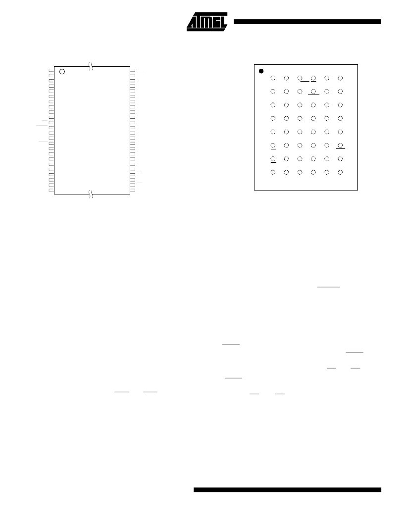
CBGA Top View
RDY/BUSY
NC
A18
NC
I/O2
I/O10
I/O11
I/O3
A3
A4
A2
A1
A0
CE
OE
VSS
A7
A17
A6
A5
I/O0
I/O8
I/O9
I/O1
WE
RESET
VPP
NC
I/O5
I/O12
VCC
I/O4
A9
A8
A10
A11
I/O7
I/O14
I/O13
I/O6
A13
A12
A14
A15
A16
BYTE
I/A-1
VSS
A
B
C
D
E
F
G
H
1
2
3
4
5
6
TSOP Top View
Type 1
1
2
3
4
5
6
7
8
9
10
11
12
13
14
15
16
17
18
19
20
21
22
23
24
48
47
46
45
44
43
42
41
40
39
38
37
36
35
34
33
32
31
30
29
28
27
26
25
A15
A14
A13
A12
A11
A10
A9
A8
NC
NC
WE
RESET
VPP
NC
RDY/BUSY
A18
A17
A7
A6
A5
A4
A3
A2
A1
A16
BYTE
GND
I/O15/A-1
I/O7
I/O14
I/O6
I/O13
I/O5
I/O12
I/O4
VCC
I/O11
I/O3
I/O10
I/O2
I/O9
I/O1
I/O8
I/O0
OE
GND
CE
A0
相关PDF资料 |
PDF描述 |
|---|---|
| AT49LV8011T | 8-megabit 3-volt Flash Memory(8M位 3V闪速存储器) |
| AT49BV802A | 8-megabit (512K x 16/ 1M x 8) 3-volt Only Flash Memory |
| AT49BV802A-70CI | 8-megabit (512K x 16/ 1M x 8) 3-volt Only Flash Memory |
| AT49BV802A-70TI | 8-megabit (512K x 16/ 1M x 8) 3-volt Only Flash Memory |
| AT49BV802AT | 8-megabit (512K x 16/ 1M x 8) 3-volt Only Flash Memory |
相关代理商/技术参数 |
参数描述 |
|---|---|
| AT49LW040-33JC | 制造商:Atmel Corporation 功能描述:NOR Flash, 512K x 8, 32 Pin, Plastic, PLCC |
| AT49LW080-33JC | 功能描述:IC FLASH 8MBIT 33MHZ 32PLCC RoHS:否 类别:集成电路 (IC) >> 存储器 系列:- 标准包装:1 系列:- 格式 - 存储器:RAM 存储器类型:SDRAM 存储容量:256M(8Mx32) 速度:143MHz 接口:并联 电源电压:3 V ~ 3.6 V 工作温度:-40°C ~ 85°C 封装/外壳:90-VFBGA 供应商设备封装:90-VFBGA(8x13) 包装:托盘 其它名称:Q2841869 |
| AT49LW080-33JC SL383 | 功能描述:IC FLASH 8MBIT 33MHZ 32PLCC RoHS:否 类别:集成电路 (IC) >> 存储器 系列:- 标准包装:1 系列:- 格式 - 存储器:RAM 存储器类型:SDRAM 存储容量:256M(8Mx32) 速度:143MHz 接口:并联 电源电压:3 V ~ 3.6 V 工作温度:-40°C ~ 85°C 封装/外壳:90-VFBGA 供应商设备封装:90-VFBGA(8x13) 包装:托盘 其它名称:Q2841869 |
| AT49LW080-33JC-T | 功能描述:IC FLASH 8MBIT 33MHZ 32PLCC 制造商:microchip technology 系列:- 包装:带卷(TR) 零件状态:停產 存储器类型:非易失 存储器格式:闪存 技术:FLASH 存储容量:8Mb (1M x 8) 时钟频率:33MHz 写周期时间 - 字,页:300μs 存储器接口:并联 电压 - 电源:3 V ~ 3.6 V 工作温度:0°C ~ 85°C(TC) 安装类型:表面贴装 封装/外壳:32-LCC(J 形引线) 供应商器件封装:32-PLCC 基本零件编号:AT49LW080 标准包装:750 |
| AT49LW080-33JX | 功能描述:IC FLASH 8MBIT 33MHZ 32PLCC RoHS:是 类别:集成电路 (IC) >> 存储器 系列:- 标准包装:1 系列:- 格式 - 存储器:RAM 存储器类型:SDRAM 存储容量:256M(8Mx32) 速度:143MHz 接口:并联 电源电压:3 V ~ 3.6 V 工作温度:-40°C ~ 85°C 封装/外壳:90-VFBGA 供应商设备封装:90-VFBGA(8x13) 包装:托盘 其它名称:Q2841869 |
发布紧急采购,3分钟左右您将得到回复。