参数资料
| 型号: | AT89C51RB2-SLRIL |
| 厂商: | Atmel |
| 文件页数: | 94/127页 |
| 文件大小: | 0K |
| 描述: | IC MCU FLASH 8051 16K 3V 44-PLCC |
| 标准包装: | 1 |
| 系列: | 89C |
| 核心处理器: | 8051 |
| 芯体尺寸: | 8-位 |
| 速度: | 40MHz |
| 连通性: | SPI,UART/USART |
| 外围设备: | POR,PWM,WDT |
| 输入/输出数: | 32 |
| 程序存储器容量: | 16KB(16K x 8) |
| 程序存储器类型: | 闪存 |
| RAM 容量: | 1.25K x 8 |
| 电压 - 电源 (Vcc/Vdd): | 2.7 V ~ 3.6 V |
| 振荡器型: | 外部 |
| 工作温度: | -40°C ~ 85°C |
| 封装/外壳: | 44-LCC(J 形引线) |
| 包装: | 剪切带 (CT) |
| 配用: | AT89STK-11-ND - KIT STARTER FOR AT89C51RX2 |
| 其它名称: | AT89C51RB2SLRILCT |
第1页第2页第3页第4页第5页第6页第7页第8页第9页第10页第11页第12页第13页第14页第15页第16页第17页第18页第19页第20页第21页第22页第23页第24页第25页第26页第27页第28页第29页第30页第31页第32页第33页第34页第35页第36页第37页第38页第39页第40页第41页第42页第43页第44页第45页第46页第47页第48页第49页第50页第51页第52页第53页第54页第55页第56页第57页第58页第59页第60页第61页第62页第63页第64页第65页第66页第67页第68页第69页第70页第71页第72页第73页第74页第75页第76页第77页第78页第79页第80页第81页第82页第83页第84页第85页第86页第87页第88页第89页第90页第91页第92页第93页当前第94页第95页第96页第97页第98页第99页第100页第101页第102页第103页第104页第105页第106页第107页第108页第109页第110页第111页第112页第113页第114页第115页第116页第117页第118页第119页第120页第121页第122页第123页第124页第125页第126页第127页
69
AT89C51RB2/RC2
4180E–8051–10/06
drive the network. The Master may select each Slave device by software through port
pins (Figure 26). To prevent bus conflicts on the MISO line, only one slave should be
selected at a time by the Master for a transmission.
In a Master configuration, the SS line can be used in conjunction with the MODF flag in
the SPI Status register (SPSTA) to prevent multiple masters from driving MOSI and
SCK (see Error conditions).
A high level on the SS pin puts the MISO line of a Slave SPI in a high-impedance state.
The SS pin could be used as a general-purpose if the following conditions are met:
The device is configured as a Master and the SSDIS control bit in SPCON is set.
This kind of configuration can be found when only one Master is driving the network
and there is no way that the SS pin could be pulled low. Therefore, the MODF flag in
the SPSTA will never be set(1).
The Device is configured as a Slave with CPHA and SSDIS control bits set
(2). This
kind of configuration can happen when the system comprises one Master and one
Slave only. Therefore, the device should always be selected and there is no reason
that the Master uses the SS pin to select the communicating Slave device.
Note:
1. Clearing SSDIS control bit does not clear MODF.
2. Special care should be taken not to set SSDIS control bit when CPHA = ’0’ because
in this mode, the SS is used to start the transmission.
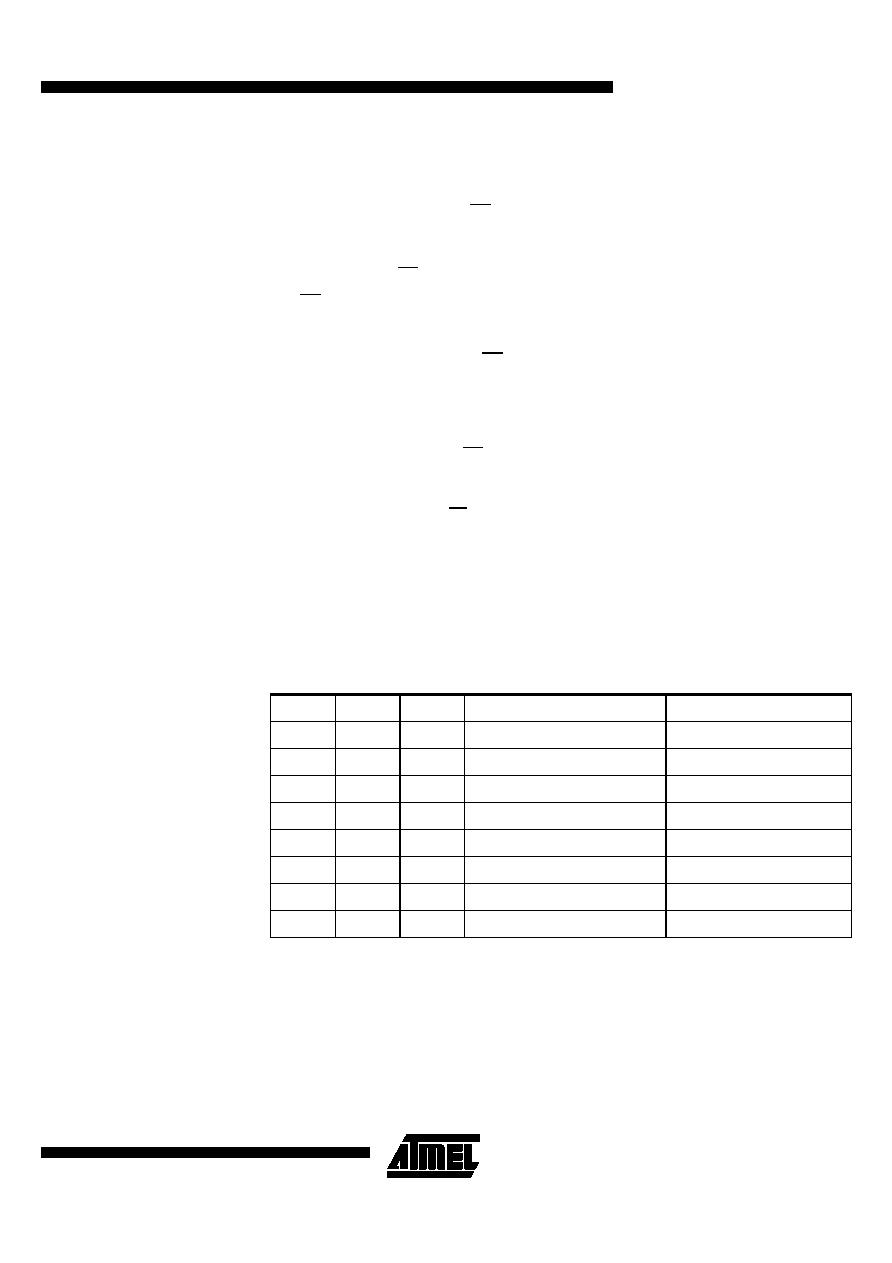
Baud Rate
In Master mode, the baud rate can be selected from a baud rate generator which is con-
trolled by three bits in the SPCON register: SPR2, SPR1 and SPR0.The Master clock is
selected from one of seven clock rates resulting from the division of the internal clock by
2, 4, 8, 16, 32, 64 or 128.
Table 54 gives the different clock rates selected by SPR2:SPR1:SPR0.
Table 54. SPI Master Baud Rate Selection
SPR2
SPR1
SPR0
Clock Rate
Baud Rate Divisor (BD)
00
0
F
CLK PERIPH /2
2
00
1
F
CLK PERIPH /4
4
01
0
F
CLK PERIPH/8
8
01
1
F
CLK PERIPH /16
16
10
0
F
CLK PERIPH /32
32
10
1
F
CLK PERIPH /64
64
11
0
F
CLK PERIPH /128
128
1
Don’t Use
No BRG
相关PDF资料 |
PDF描述 |
|---|---|
| AT89C51ID2-SLRIM | IC MCU FLASH 8051 64K 5V 44-PLCC |
| PIC16C923-04/L | IC MCU OTP 4KX14 LCD DVR 68PLCC |
| PIC18F2423-I/SO | IC PIC MCU FLASH 8KX16 28SOIC |
| PIC16C57-LP/SO | IC MCU OTP 2KX12 28SOIC |
| PIC18LF6410-I/PT | IC PIC MCU FLASH 8KX16 64TQFP |
相关代理商/技术参数 |
参数描述 |
|---|---|
| AT89C51RB2-SLRIM | 功能描述:IC MCU FLASH 8051 16K 5V 44-PLCC RoHS:否 类别:集成电路 (IC) >> 嵌入式 - 微控制器, 系列:89C 标准包装:1,500 系列:AVR® ATtiny 核心处理器:AVR 芯体尺寸:8-位 速度:16MHz 连通性:I²C,LIN,SPI,UART/USART,USI 外围设备:欠压检测/复位,POR,PWM,温度传感器,WDT 输入/输出数:16 程序存储器容量:8KB(4K x 16) 程序存储器类型:闪存 EEPROM 大小:512 x 8 RAM 容量:512 x 8 电压 - 电源 (Vcc/Vdd):2.7 V ~ 5.5 V 数据转换器:A/D 11x10b 振荡器型:内部 工作温度:-40°C ~ 125°C 封装/外壳:20-SOIC(0.295",7.50mm 宽) 包装:带卷 (TR) |
| AT89C51RB2-SLRUL | 功能描述:8位微控制器 -MCU C51RB2 FLASH 3V 16k Ind RoHS:否 制造商:Silicon Labs 核心:8051 处理器系列:C8051F39x 数据总线宽度:8 bit 最大时钟频率:50 MHz 程序存储器大小:16 KB 数据 RAM 大小:1 KB 片上 ADC:Yes 工作电源电压:1.8 V to 3.6 V 工作温度范围:- 40 C to + 105 C 封装 / 箱体:QFN-20 安装风格:SMD/SMT |
| AT89C51RB2-SLRUM | 功能描述:8位微控制器 -MCU C51RB2 FLASH 5V 16k ind RoHS:否 制造商:Silicon Labs 核心:8051 处理器系列:C8051F39x 数据总线宽度:8 bit 最大时钟频率:50 MHz 程序存储器大小:16 KB 数据 RAM 大小:1 KB 片上 ADC:Yes 工作电源电压:1.8 V to 3.6 V 工作温度范围:- 40 C to + 105 C 封装 / 箱体:QFN-20 安装风格:SMD/SMT |
| AT89C51RB2-SLSCM | 制造商:ATMEL 制造商全称:ATMEL Corporation 功能描述:Microcontroller with 16K/32K Bytes Flash |
| AT89C51RB2-SLSIL | 功能描述:IC 8051 MCU FLASH 16K 44PLCC RoHS:否 类别:集成电路 (IC) >> 嵌入式 - 微控制器, 系列:89C 标准包装:9 系列:87C 核心处理器:8051 芯体尺寸:8-位 速度:40/20MHz 连通性:UART/USART 外围设备:POR,WDT 输入/输出数:32 程序存储器容量:32KB(32K x 8) 程序存储器类型:OTP EEPROM 大小:- RAM 容量:256 x 8 电压 - 电源 (Vcc/Vdd):4.5 V ~ 5.5 V 数据转换器:- 振荡器型:内部 工作温度:0°C ~ 70°C 封装/外壳:40-DIP(0.600",15.24mm) 包装:管件 |
发布紧急采购,3分钟左右您将得到回复。