- 您现在的位置:买卖IC网 > PDF目录11723 > AT89LP213-20PU (Atmel)MCU 8051 2K FLASH 20MHZ 14-PDIP PDF资料下载
参数资料
| 型号: | AT89LP213-20PU |
| 厂商: | Atmel |
| 文件页数: | 27/98页 |
| 文件大小: | 0K |
| 描述: | MCU 8051 2K FLASH 20MHZ 14-PDIP |
| 产品培训模块: | MCU Product Line Introduction |
| 标准包装: | 25 |
| 系列: | 89LP |
| 核心处理器: | 8051 |
| 芯体尺寸: | 8-位 |
| 速度: | 20MHz |
| 连通性: | SPI |
| 外围设备: | 欠压检测/复位,POR,PWM,WDT |
| 输入/输出数: | 12 |
| 程序存储器容量: | 2KB(2K x 8) |
| 程序存储器类型: | 闪存 |
| RAM 容量: | 128 x 8 |
| 电压 - 电源 (Vcc/Vdd): | 2.4 V ~ 5.5 V |
| 振荡器型: | 内部 |
| 工作温度: | -40°C ~ 85°C |
| 封装/外壳: | 14-DIP(0.300",7.62mm) |
| 包装: | 管件 |
第1页第2页第3页第4页第5页第6页第7页第8页第9页第10页第11页第12页第13页第14页第15页第16页第17页第18页第19页第20页第21页第22页第23页第24页第25页第26页当前第27页第28页第29页第30页第31页第32页第33页第34页第35页第36页第37页第38页第39页第40页第41页第42页第43页第44页第45页第46页第47页第48页第49页第50页第51页第52页第53页第54页第55页第56页第57页第58页第59页第60页第61页第62页第63页第64页第65页第66页第67页第68页第69页第70页第71页第72页第73页第74页第75页第76页第77页第78页第79页第80页第81页第82页第83页第84页第85页第86页第87页第88页第89页第90页第91页第92页第93页第94页第95页第96页第97页第98页
33
3538E–MICRO–11/10
AT89LP213/214
.
14.5
Pulse Width Modulation
On the AT89LP213, Timer 0 and Timer 1 may be independently configured as 8-bit asymmetri-
cal (edge-aligned) pulse width modulators (PWM) by setting the PWM0EN or PWM1EN bits in
TCONB, respectively. In PWM Mode the generated waveform is output on the timer's input pin,
T0 or T1. Therefore, C/T must be set to “0” when in PWM mode. and the T0 (P3.4) and T1 (P3.5)
must be configured in an output mode. The Timer Overflow Flags and Interrupts will continue to
function while in PWM Mode and Timer 1 may still generate the baud rate for the UART. Each
PWM channel has four modes selected by the mode bits in TMOD.
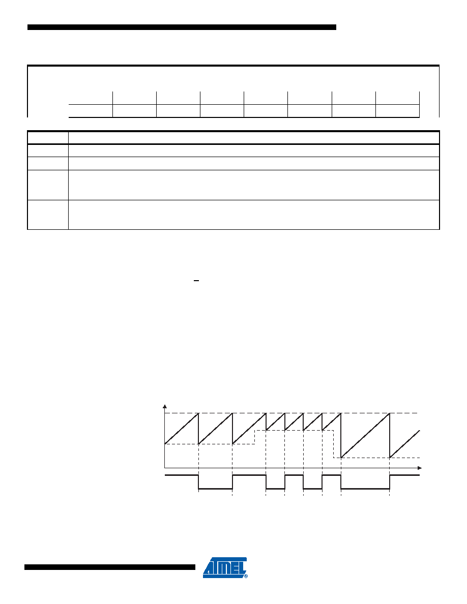
An example waveform for Timer 0 in PWM Mode 0 is shown in Figure 14-5. TH0 acts as an 8-bit
counter while RH0 stores the 8-bit compare value. When TH0 is 00H the PWM output is
set high. When the TH0 count reaches the value stored in RH0 the PWM output is set low.
Therefore, the pulse width is proportional to the value in RH0. To prevent glitches, writes to
RH0 only take effect on the FFH to 00H overflow of TH0. Setting RH0 to 00H will keep the PWM
output low.
Figure 14-5. Asymmetrical Pulse Width Modulation
Table 14-3.
TCONB
– Timer/Counter Control Register B
TCONB = 91H
Reset Value = 0010 0100B
Not Bit Addressable
PWM1EN
PWM0EN
PSC12
PSC11
PSC10
PSC02
PSC01
PSC00
Bit
7
6
543
21
0
Symbol
Function
PWM1EN
Configures Timer 1 for Pulse Width Modulation output on T1 (P3.5).
PWM0EN
Configures Timer 0 for Pulse Width Modulation output on T0 (P3.4).
PSC12
PSC11
PSC10
Prescaler for Timer 1 Mode 0. The number of active bits in TL1 equals PSC1 + 1. After reset PSC1 = 100B which
enables 5 bits of TL1 for compatibility with the 13-bit Mode 0 in AT89S2051.
PSC02
PSC01
PSC00
Prescaler for Timer 0 Mode 0. The number of active bits in TL0 equals PSC0 + 1. After reset PSC0 = 100B which
enables 5 bits of TL0 for compatibility with the 13-bit Mode 0 in AT89C52.
Tx
THx
FFh
相关PDF资料 |
PDF描述 |
|---|---|
| VE-B5X-IX-F4 | CONVERTER MOD DC/DC 5.2V 75W |
| V375A36E500BG | CONVERTER MOD DC/DC 36V 500W |
| AT89LP214-20XU | MCU 8051 2K FLASH 20MHZ 14-TSSOP |
| VE-B5X-IW-F2 | CONVERTER MOD DC/DC 5.2V 100W |
| V375A36E500BF3 | CONVERTER MOD DC/DC 36V 500W |
相关代理商/技术参数 |
参数描述 |
|---|---|
| AT89LP213-20SU | 功能描述:8位微控制器 -MCU SINGLE CYCLE 2K ISP FLASH 2.4-5.5V RoHS:否 制造商:Silicon Labs 核心:8051 处理器系列:C8051F39x 数据总线宽度:8 bit 最大时钟频率:50 MHz 程序存储器大小:16 KB 数据 RAM 大小:1 KB 片上 ADC:Yes 工作电源电压:1.8 V to 3.6 V 工作温度范围:- 40 C to + 105 C 封装 / 箱体:QFN-20 安装风格:SMD/SMT |
| AT89LP213-20XU | 功能描述:8位微控制器 -MCU SINGLE CYCLE 2K ISP FLASH 2.4-5.5V RoHS:否 制造商:Silicon Labs 核心:8051 处理器系列:C8051F39x 数据总线宽度:8 bit 最大时钟频率:50 MHz 程序存储器大小:16 KB 数据 RAM 大小:1 KB 片上 ADC:Yes 工作电源电压:1.8 V to 3.6 V 工作温度范围:- 40 C to + 105 C 封装 / 箱体:QFN-20 安装风格:SMD/SMT |
| AT89LP214-16XI | 功能描述:8位微控制器 -MCU Microcontroller RoHS:否 制造商:Silicon Labs 核心:8051 处理器系列:C8051F39x 数据总线宽度:8 bit 最大时钟频率:50 MHz 程序存储器大小:16 KB 数据 RAM 大小:1 KB 片上 ADC:Yes 工作电源电压:1.8 V to 3.6 V 工作温度范围:- 40 C to + 105 C 封装 / 箱体:QFN-20 安装风格:SMD/SMT |
| AT89LP214-20PU | 功能描述:8位微控制器 -MCU SINGLE CYCLE 2K ISP FLASH 2.4-5.5V RoHS:否 制造商:Silicon Labs 核心:8051 处理器系列:C8051F39x 数据总线宽度:8 bit 最大时钟频率:50 MHz 程序存储器大小:16 KB 数据 RAM 大小:1 KB 片上 ADC:Yes 工作电源电压:1.8 V to 3.6 V 工作温度范围:- 40 C to + 105 C 封装 / 箱体:QFN-20 安装风格:SMD/SMT |
| AT89LP214-20SU | 功能描述:8位微控制器 -MCU SINGLE CYCLE 2K ISP FLASH 2.4-5.5V RoHS:否 制造商:Silicon Labs 核心:8051 处理器系列:C8051F39x 数据总线宽度:8 bit 最大时钟频率:50 MHz 程序存储器大小:16 KB 数据 RAM 大小:1 KB 片上 ADC:Yes 工作电源电压:1.8 V to 3.6 V 工作温度范围:- 40 C to + 105 C 封装 / 箱体:QFN-20 安装风格:SMD/SMT |
发布紧急采购,3分钟左右您将得到回复。