- 您现在的位置:买卖IC网 > PDF目录11724 > AT89LP213-20XU (Atmel)MCU 8051 2K FLASH 20MHZ 14-TSSOP PDF资料下载
参数资料
| 型号: | AT89LP213-20XU |
| 厂商: | Atmel |
| 文件页数: | 5/98页 |
| 文件大小: | 0K |
| 描述: | MCU 8051 2K FLASH 20MHZ 14-TSSOP |
| 产品培训模块: | MCU Product Line Introduction |
| 标准包装: | 95 |
| 系列: | 89LP |
| 核心处理器: | 8051 |
| 芯体尺寸: | 8-位 |
| 速度: | 20MHz |
| 连通性: | SPI |
| 外围设备: | 欠压检测/复位,POR,PWM,WDT |
| 输入/输出数: | 12 |
| 程序存储器容量: | 2KB(2K x 8) |
| 程序存储器类型: | 闪存 |
| RAM 容量: | 128 x 8 |
| 电压 - 电源 (Vcc/Vdd): | 2.4 V ~ 5.5 V |
| 振荡器型: | 内部 |
| 工作温度: | -40°C ~ 85°C |
| 封装/外壳: | 14-TSSOP(0.173",4.40mm 宽) |
| 包装: | 管件 |
第1页第2页第3页第4页当前第5页第6页第7页第8页第9页第10页第11页第12页第13页第14页第15页第16页第17页第18页第19页第20页第21页第22页第23页第24页第25页第26页第27页第28页第29页第30页第31页第32页第33页第34页第35页第36页第37页第38页第39页第40页第41页第42页第43页第44页第45页第46页第47页第48页第49页第50页第51页第52页第53页第54页第55页第56页第57页第58页第59页第60页第61页第62页第63页第64页第65页第66页第67页第68页第69页第70页第71页第72页第73页第74页第75页第76页第77页第78页第79页第80页第81页第82页第83页第84页第85页第86页第87页第88页第89页第90页第91页第92页第93页第94页第95页第96页第97页第98页
13
3538E–MICRO–11/10
AT89LP213/214
9.2
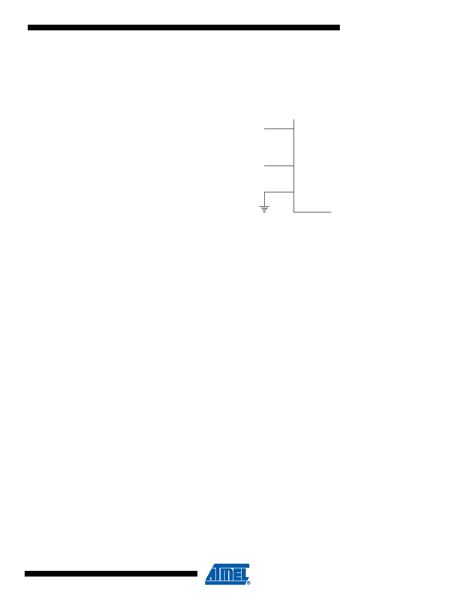
External Clock Source
The external clock option disables the oscillator amplifier and allows XTAL1 to be driven directly
by the clock source as shown in Figure 9-2. XTAL2 may be left unconnected, used as P3.3 I/O,
or configured to output a divided version of the system clock.
Figure 9-2.
External Clock Drive Configuration
9.3
Internal RC Oscillator
The AT89LP213/214 has an internal RC oscillator tuned to 8.0 MHz ±1.0% at 5.0V and 25
° C.
When enabled as the clock source, XTAL1 and XTAL2 may be used as P3.2 and P3.3 respec-
tively. XTAL2 may also be configured to output a divided version of the system clock. The
frequency of the oscillator may be adjusted by changing the RC Adjust Fuses. (See “User Con-
figuration Fuses” on page 72). A copy of the initial factory setting is stored at location 0007h of
the Atmel SIgnature.
9.4
System Clock Out
When the AT89LP213/214 is configured to use either an external clock or the internal RC oscil-
lator, a divided version of the system clock may be output on XTAL2 (P3.3). The Clock Out
feature is enabled by setting the COE bit in CLKREG. The two CDV bits determine the clock
divide ratio. For example, setting COE = “1” and CDIV = “00” when using the internal oscillator
will result in a 4.0 MHz clock output on P3.3. P3.3 must be configured as an output in order to
use the clock out feature.
XTAL2 (P3.3)
XTAL1 (P3.2)
GND
NC, GPIO, or
CLKOUT
EXTERNAL
OSCILLATOR
SIGNAL
相关PDF资料 |
PDF描述 |
|---|---|
| V375A36E500BF2 | CONVERTER MOD DC/DC 36V 500W |
| V375A36E500BF | CONVERTER MOD DC/DC 36V 500W |
| V375A36E500BL3 | CONVERTER MOD DC/DC 36V 500W |
| 31-212 | BNC CONN CLAMP/SOLDER RG-59 |
| V375A36E500BL | CONVERTER MOD DC/DC 36V 500W |
相关代理商/技术参数 |
参数描述 |
|---|---|
| AT89LP214-16XI | 功能描述:8位微控制器 -MCU Microcontroller RoHS:否 制造商:Silicon Labs 核心:8051 处理器系列:C8051F39x 数据总线宽度:8 bit 最大时钟频率:50 MHz 程序存储器大小:16 KB 数据 RAM 大小:1 KB 片上 ADC:Yes 工作电源电压:1.8 V to 3.6 V 工作温度范围:- 40 C to + 105 C 封装 / 箱体:QFN-20 安装风格:SMD/SMT |
| AT89LP214-20PU | 功能描述:8位微控制器 -MCU SINGLE CYCLE 2K ISP FLASH 2.4-5.5V RoHS:否 制造商:Silicon Labs 核心:8051 处理器系列:C8051F39x 数据总线宽度:8 bit 最大时钟频率:50 MHz 程序存储器大小:16 KB 数据 RAM 大小:1 KB 片上 ADC:Yes 工作电源电压:1.8 V to 3.6 V 工作温度范围:- 40 C to + 105 C 封装 / 箱体:QFN-20 安装风格:SMD/SMT |
| AT89LP214-20SU | 功能描述:8位微控制器 -MCU SINGLE CYCLE 2K ISP FLASH 2.4-5.5V RoHS:否 制造商:Silicon Labs 核心:8051 处理器系列:C8051F39x 数据总线宽度:8 bit 最大时钟频率:50 MHz 程序存储器大小:16 KB 数据 RAM 大小:1 KB 片上 ADC:Yes 工作电源电压:1.8 V to 3.6 V 工作温度范围:- 40 C to + 105 C 封装 / 箱体:QFN-20 安装风格:SMD/SMT |
| AT89LP214-20XU | 功能描述:8位微控制器 -MCU SINGLE CYCLE 2K ISP FLASH 2.4-5.5V RoHS:否 制造商:Silicon Labs 核心:8051 处理器系列:C8051F39x 数据总线宽度:8 bit 最大时钟频率:50 MHz 程序存储器大小:16 KB 数据 RAM 大小:1 KB 片上 ADC:Yes 工作电源电压:1.8 V to 3.6 V 工作温度范围:- 40 C to + 105 C 封装 / 箱体:QFN-20 安装风格:SMD/SMT |
| AT89LP216-16XI | 功能描述:8位微控制器 -MCU Microcontroller RoHS:否 制造商:Silicon Labs 核心:8051 处理器系列:C8051F39x 数据总线宽度:8 bit 最大时钟频率:50 MHz 程序存储器大小:16 KB 数据 RAM 大小:1 KB 片上 ADC:Yes 工作电源电压:1.8 V to 3.6 V 工作温度范围:- 40 C to + 105 C 封装 / 箱体:QFN-20 安装风格:SMD/SMT |
发布紧急采购,3分钟左右您将得到回复。