- 您现在的位置:买卖IC网 > PDF目录11724 > AT89LP213-20XU (Atmel)MCU 8051 2K FLASH 20MHZ 14-TSSOP PDF资料下载
参数资料
| 型号: | AT89LP213-20XU |
| 厂商: | Atmel |
| 文件页数: | 64/98页 |
| 文件大小: | 0K |
| 描述: | MCU 8051 2K FLASH 20MHZ 14-TSSOP |
| 产品培训模块: | MCU Product Line Introduction |
| 标准包装: | 95 |
| 系列: | 89LP |
| 核心处理器: | 8051 |
| 芯体尺寸: | 8-位 |
| 速度: | 20MHz |
| 连通性: | SPI |
| 外围设备: | 欠压检测/复位,POR,PWM,WDT |
| 输入/输出数: | 12 |
| 程序存储器容量: | 2KB(2K x 8) |
| 程序存储器类型: | 闪存 |
| RAM 容量: | 128 x 8 |
| 电压 - 电源 (Vcc/Vdd): | 2.4 V ~ 5.5 V |
| 振荡器型: | 内部 |
| 工作温度: | -40°C ~ 85°C |
| 封装/外壳: | 14-TSSOP(0.173",4.40mm 宽) |
| 包装: | 管件 |
第1页第2页第3页第4页第5页第6页第7页第8页第9页第10页第11页第12页第13页第14页第15页第16页第17页第18页第19页第20页第21页第22页第23页第24页第25页第26页第27页第28页第29页第30页第31页第32页第33页第34页第35页第36页第37页第38页第39页第40页第41页第42页第43页第44页第45页第46页第47页第48页第49页第50页第51页第52页第53页第54页第55页第56页第57页第58页第59页第60页第61页第62页第63页当前第64页第65页第66页第67页第68页第69页第70页第71页第72页第73页第74页第75页第76页第77页第78页第79页第80页第81页第82页第83页第84页第85页第86页第87页第88页第89页第90页第91页第92页第93页第94页第95页第96页第97页第98页
67
3538E–MICRO–11/10
AT89LP213/214
driven low prior to the end of Power-On Reset (POR). After POR has completed the device
will remain in ISP mode until RST is brought high. Once the initial ISP session has ended, the
power to the target device must be cycled OFF and ON to enter another session.
The SS pin should not be left floating during reset if ISP is enabled.
The ISP Enable Fuse must be set to allow programming during any reset period. If the ISP
Fuse is disabled, ISP may only be entered at POR.
23.2
Memory Organization
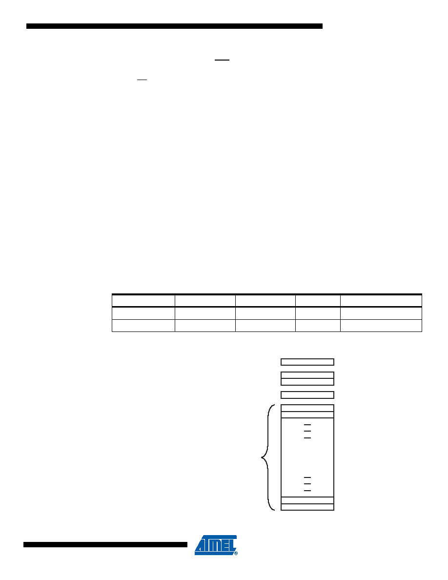
The AT89LP213/214 offers 2K bytes of In-System Programmable (ISP) nonvolatile Flash code
memory. In addition, the device contains a 64-byte User Signature Array and a 32-byte read-
only Atmel Signature Array. The memory organization is shown in Table 23-1 and Figure 23-2.
The memory is divided into pages of 32 bytes each. A single read or write command may only
access a single page in the memory. Each memory type resides in its own address space and is
accessed by commands specific to that memory. However, all memory types share the same
page size.
User configuration fuses are mapped as a row in the memory, with each byte representing one
fuse. From a programming standpoint, fuses are treated the same as normal code bytes except
they are not affected by Chip Erase. Fuses can be enabled at any time by writing 00h to the
appropriate locations in the fuse row. However, to disable a fuse, i.e. set it to FFh, the entire
fuse row must be erased and then reprogrammed. The programmer should read the state of all
the fuses into a temporary location, modify those fuses which need to be disabled, then issue a
Fuse Write with Auto-Erase command using the temporary data. Lock bits are treated in a simi-
lar manner to fuses except they may only be erased (unlocked) by Chip Erase.
Figure 23-2. AT89LP213/214 Memory Organization
Table 23-1.
Code Memory Sizes
Device #
Code Size
Page Size
# Pages
Address Range
AT89LP213
2K bytes
32 bytes
64
0000H - 07FFH
AT89LP214
2K bytes
32 bytes
64
0000H - 07FFH
Page 0
Page 1
Page 63
Page 62
Page 0
User Fuse Row
User Signature Array
Atmel Signature Array
Code Memory
Page 1
00
1F
0000
07FF
相关PDF资料 |
PDF描述 |
|---|---|
| V375A36E500BF2 | CONVERTER MOD DC/DC 36V 500W |
| V375A36E500BF | CONVERTER MOD DC/DC 36V 500W |
| V375A36E500BL3 | CONVERTER MOD DC/DC 36V 500W |
| 31-212 | BNC CONN CLAMP/SOLDER RG-59 |
| V375A36E500BL | CONVERTER MOD DC/DC 36V 500W |
相关代理商/技术参数 |
参数描述 |
|---|---|
| AT89LP214-16XI | 功能描述:8位微控制器 -MCU Microcontroller RoHS:否 制造商:Silicon Labs 核心:8051 处理器系列:C8051F39x 数据总线宽度:8 bit 最大时钟频率:50 MHz 程序存储器大小:16 KB 数据 RAM 大小:1 KB 片上 ADC:Yes 工作电源电压:1.8 V to 3.6 V 工作温度范围:- 40 C to + 105 C 封装 / 箱体:QFN-20 安装风格:SMD/SMT |
| AT89LP214-20PU | 功能描述:8位微控制器 -MCU SINGLE CYCLE 2K ISP FLASH 2.4-5.5V RoHS:否 制造商:Silicon Labs 核心:8051 处理器系列:C8051F39x 数据总线宽度:8 bit 最大时钟频率:50 MHz 程序存储器大小:16 KB 数据 RAM 大小:1 KB 片上 ADC:Yes 工作电源电压:1.8 V to 3.6 V 工作温度范围:- 40 C to + 105 C 封装 / 箱体:QFN-20 安装风格:SMD/SMT |
| AT89LP214-20SU | 功能描述:8位微控制器 -MCU SINGLE CYCLE 2K ISP FLASH 2.4-5.5V RoHS:否 制造商:Silicon Labs 核心:8051 处理器系列:C8051F39x 数据总线宽度:8 bit 最大时钟频率:50 MHz 程序存储器大小:16 KB 数据 RAM 大小:1 KB 片上 ADC:Yes 工作电源电压:1.8 V to 3.6 V 工作温度范围:- 40 C to + 105 C 封装 / 箱体:QFN-20 安装风格:SMD/SMT |
| AT89LP214-20XU | 功能描述:8位微控制器 -MCU SINGLE CYCLE 2K ISP FLASH 2.4-5.5V RoHS:否 制造商:Silicon Labs 核心:8051 处理器系列:C8051F39x 数据总线宽度:8 bit 最大时钟频率:50 MHz 程序存储器大小:16 KB 数据 RAM 大小:1 KB 片上 ADC:Yes 工作电源电压:1.8 V to 3.6 V 工作温度范围:- 40 C to + 105 C 封装 / 箱体:QFN-20 安装风格:SMD/SMT |
| AT89LP216-16XI | 功能描述:8位微控制器 -MCU Microcontroller RoHS:否 制造商:Silicon Labs 核心:8051 处理器系列:C8051F39x 数据总线宽度:8 bit 最大时钟频率:50 MHz 程序存储器大小:16 KB 数据 RAM 大小:1 KB 片上 ADC:Yes 工作电源电压:1.8 V to 3.6 V 工作温度范围:- 40 C to + 105 C 封装 / 箱体:QFN-20 安装风格:SMD/SMT |
发布紧急采购,3分钟左右您将得到回复。