- 您现在的位置:买卖IC网 > PDF目录11724 > AT89LP213-20XU (Atmel)MCU 8051 2K FLASH 20MHZ 14-TSSOP PDF资料下载
参数资料
| 型号: | AT89LP213-20XU |
| 厂商: | Atmel |
| 文件页数: | 78/98页 |
| 文件大小: | 0K |
| 描述: | MCU 8051 2K FLASH 20MHZ 14-TSSOP |
| 产品培训模块: | MCU Product Line Introduction |
| 标准包装: | 95 |
| 系列: | 89LP |
| 核心处理器: | 8051 |
| 芯体尺寸: | 8-位 |
| 速度: | 20MHz |
| 连通性: | SPI |
| 外围设备: | 欠压检测/复位,POR,PWM,WDT |
| 输入/输出数: | 12 |
| 程序存储器容量: | 2KB(2K x 8) |
| 程序存储器类型: | 闪存 |
| RAM 容量: | 128 x 8 |
| 电压 - 电源 (Vcc/Vdd): | 2.4 V ~ 5.5 V |
| 振荡器型: | 内部 |
| 工作温度: | -40°C ~ 85°C |
| 封装/外壳: | 14-TSSOP(0.173",4.40mm 宽) |
| 包装: | 管件 |
第1页第2页第3页第4页第5页第6页第7页第8页第9页第10页第11页第12页第13页第14页第15页第16页第17页第18页第19页第20页第21页第22页第23页第24页第25页第26页第27页第28页第29页第30页第31页第32页第33页第34页第35页第36页第37页第38页第39页第40页第41页第42页第43页第44页第45页第46页第47页第48页第49页第50页第51页第52页第53页第54页第55页第56页第57页第58页第59页第60页第61页第62页第63页第64页第65页第66页第67页第68页第69页第70页第71页第72页第73页第74页第75页第76页第77页当前第78页第79页第80页第81页第82页第83页第84页第85页第86页第87页第88页第89页第90页第91页第92页第93页第94页第95页第96页第97页第98页
8
3538E–MICRO–11/10
AT89LP213/214
A map of the AT89LP213/214 program memory is shown in Figure 6-1. In addition to the 2K
code space from 0000h to 07FFh, the AT89LP213/214 also supports a 64-byte User Signature
Array and a 32-byte Atmel Signature Array that are accessible by the CPU in a read-only fash-
ion. In order to read from the signature arrays, the SIGEN bit in AUXR1 must be set. While
SIGEN is one, MOVC A,@A+DPTR will access the signature arrays. The User Signature Array
is mapped to addresses 0040h to 007Fh and the Atmel Signature Array is mapped to addresses
0000h to 001Fh. SIGEN must be cleared before using MOVC to access the code memory.
The Atmel Signature Array is initialized with the Device ID in the factory. The User Signature
Array is available for user identification codes or constant parameter data. Data stored in the sig-
nature array is not secure. Security bits will disable writes to the array; however, reads are
always allowed.
6.2
Data Memory
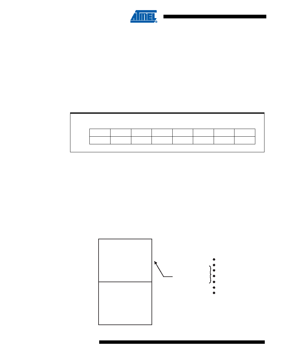
The AT89LP213/214 contains 128 bytes of general SRAM data memory plus 128 bytes of I/O
memory mapped into a single 8-bit address space. The 128 bytes of data memory may be
accessed through both direct and indirect addressing of the lower 128 byte addresses. The 128
bytes of I/O memory reside in the upper 128 byte address space (Figure 6-2). The I/O memory
can only be accessed through direct addressing and contains the Special Function Registers
(SFRs). Indirect accesses to the upper 128 byte addresses will return invalid data. The lowest
32 bytes of data memory are grouped into 4 banks of 8 registers each. The RS0 and RS1 bits
(PSW.3 and PSW.4) select which register bank is in use. Instructions using register addressing
will only access the currently specified bank. The AT89LP213/214 does not support external
data memory.
Figure 6-2.
Data Memory Map
Table 6-1.
AUXR1
– Auxiliary Register 1
AUXR1 = A2H
Reset Value = XXXX 0XXXB
Not Bit Addressable
––––
SIGEN
–––
Bit
76543
210
FFH
UPPER
128
80H
7F H
LO WER
128
0
Accessible
By Direct
Addressing
Only
Accessible
By Direct
and Indirect
Addressing
Only
Special Function
Registers
Ports
Status and Control Bits
Timers
Registers
Stack Pointer
Accumulator
(Etc.)
相关PDF资料 |
PDF描述 |
|---|---|
| V375A36E500BF2 | CONVERTER MOD DC/DC 36V 500W |
| V375A36E500BF | CONVERTER MOD DC/DC 36V 500W |
| V375A36E500BL3 | CONVERTER MOD DC/DC 36V 500W |
| 31-212 | BNC CONN CLAMP/SOLDER RG-59 |
| V375A36E500BL | CONVERTER MOD DC/DC 36V 500W |
相关代理商/技术参数 |
参数描述 |
|---|---|
| AT89LP214-16XI | 功能描述:8位微控制器 -MCU Microcontroller RoHS:否 制造商:Silicon Labs 核心:8051 处理器系列:C8051F39x 数据总线宽度:8 bit 最大时钟频率:50 MHz 程序存储器大小:16 KB 数据 RAM 大小:1 KB 片上 ADC:Yes 工作电源电压:1.8 V to 3.6 V 工作温度范围:- 40 C to + 105 C 封装 / 箱体:QFN-20 安装风格:SMD/SMT |
| AT89LP214-20PU | 功能描述:8位微控制器 -MCU SINGLE CYCLE 2K ISP FLASH 2.4-5.5V RoHS:否 制造商:Silicon Labs 核心:8051 处理器系列:C8051F39x 数据总线宽度:8 bit 最大时钟频率:50 MHz 程序存储器大小:16 KB 数据 RAM 大小:1 KB 片上 ADC:Yes 工作电源电压:1.8 V to 3.6 V 工作温度范围:- 40 C to + 105 C 封装 / 箱体:QFN-20 安装风格:SMD/SMT |
| AT89LP214-20SU | 功能描述:8位微控制器 -MCU SINGLE CYCLE 2K ISP FLASH 2.4-5.5V RoHS:否 制造商:Silicon Labs 核心:8051 处理器系列:C8051F39x 数据总线宽度:8 bit 最大时钟频率:50 MHz 程序存储器大小:16 KB 数据 RAM 大小:1 KB 片上 ADC:Yes 工作电源电压:1.8 V to 3.6 V 工作温度范围:- 40 C to + 105 C 封装 / 箱体:QFN-20 安装风格:SMD/SMT |
| AT89LP214-20XU | 功能描述:8位微控制器 -MCU SINGLE CYCLE 2K ISP FLASH 2.4-5.5V RoHS:否 制造商:Silicon Labs 核心:8051 处理器系列:C8051F39x 数据总线宽度:8 bit 最大时钟频率:50 MHz 程序存储器大小:16 KB 数据 RAM 大小:1 KB 片上 ADC:Yes 工作电源电压:1.8 V to 3.6 V 工作温度范围:- 40 C to + 105 C 封装 / 箱体:QFN-20 安装风格:SMD/SMT |
| AT89LP216-16XI | 功能描述:8位微控制器 -MCU Microcontroller RoHS:否 制造商:Silicon Labs 核心:8051 处理器系列:C8051F39x 数据总线宽度:8 bit 最大时钟频率:50 MHz 程序存储器大小:16 KB 数据 RAM 大小:1 KB 片上 ADC:Yes 工作电源电压:1.8 V to 3.6 V 工作温度范围:- 40 C to + 105 C 封装 / 箱体:QFN-20 安装风格:SMD/SMT |
发布紧急采购,3分钟左右您将得到回复。