- 您现在的位置:买卖IC网 > PDF目录42902 > ATF-34143-TR1G X BAND, Si, N-CHANNEL, RF SMALL SIGNAL, HEMFET PDF资料下载
参数资料
| 型号: | ATF-34143-TR1G |
| 元件分类: | 小信号晶体管 |
| 英文描述: | X BAND, Si, N-CHANNEL, RF SMALL SIGNAL, HEMFET |
| 封装: | LEAD FREE, PLASTIC, SC-70, 4 PIN |
| 文件页数: | 12/15页 |
| 文件大小: | 258K |
| 代理商: | ATF-34143-TR1G |
6
ATF-34143 Power Parameters tuned for Power, VDS = 4 V, IDSQ = 120 mA
Freq
(GHz)
P1dB
(dBm)
Id
(mA)
G1dB
(dB)
PAE1dB
(%)
P3dBm
(dBm)
Id
(mA)
PAE3dB
(%)
Gamma
Out_mag
(Mag)
Gamma
Out_ang
(Degrees)
0.9
20.9
114
25.7
27
22.8
108
44
0.34
136
1.5
21.7
115
21.9
32
23.1
95
53
0.31
152
1.8
21.3
111
20.5
30
23.0
105
47
0.30
164
2
22.0
106
19.5
37
23.7
115
50
0.28
171
4
22.7
110
12.7
40
23.6
111
47
0.26
-135
6
23.3
115
9.2
41
24.2
121
44
0.24
-66
ATF-34143 Power Parameters tuned for Power, VDS = 4 V, IDSQ = 60 mA
Freq
(GHz)
P1dB
(dBm)
Id
(mA)
G1dB
(dB)
PAE1dB
(%)
P3dBm
(dBm)
Id
(mA)
PAE3dB
(%)
Gamma
Out_mag
(Mag)
Gamma
Out_ang
(Degrees)
0.9
18.2
75
27.5
22
20.5
78
36
0.48
102
1.5
18.7
58
24.5
32
20.8
59
51
0.45
117
1.8
18.8
57
23.0
33
21.1
71
45
0.42
126
2
18.8
59
22.2
32
21.9
81
47
0.40
131
4
20.2
66
13.9
38
22.0
77
48
0.25
-162
6
21.2
79
9.9
37
23.5
102
46
0.18
-77
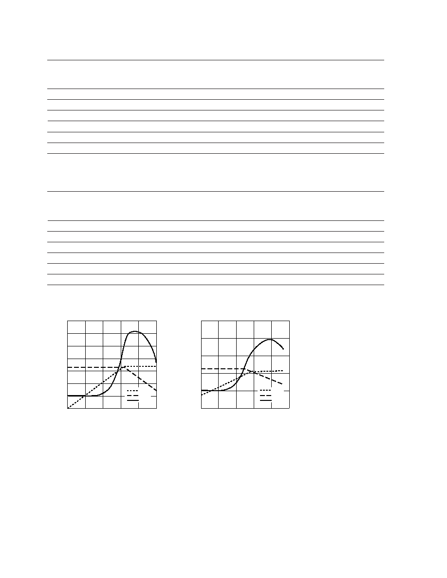
Pin (dBm)
Figure 20. Swept Power Tuned for
Power at 2 GHz, VDS= 4 V, IDSQ = 120 mA.
P
out
(dBm),
G
(dB),
PAE
(%)
-30
-10
-20
10
0
20
80
50
40
30
20
10
0
-10
Pout
Gain
PAE
Pin (dBm)
Figure 21. Swept Power Tuned for
Power at 2 GHz, VDS = 4 V, IDSQ = 60 mA.
P
out
(dBm),
G
(dB),
PAE
(%)
-30
-10
-20
10
0
20
80
60
40
20
0
-20
Pout
Gain
PAE
Notes:
1. P1dB measurements are performed with passive biasing. Quicescent drain current, IDSQ, is set with zero RF drive applied. As P1dB is approached,
the drain current may increase or decrease depending on frequency and dc bias point. At lower values of IDSQ the device is running closer to class
B as power output approaches P1dB. This results in higher PAE (power added efficiency) when compared to a device that is driven by a constant
current source as is typically done with active biasing. As an example, at a VDS = 4 V and IDSQ = 10 mA, Id increases to 62 mA as a P1dB of +19 dBm
is approached.
2. PAE(%) = ((Pout – Pin)/Pdc) x 100
3. Gamma out is the reflection coefficient of the matching circuit presented to the output of the device.
相关PDF资料 |
PDF描述 |
|---|---|
| ATF-34143-BLKG | X BAND, Si, N-CHANNEL, RF SMALL SIGNAL, HEMFET |
| ATF-34143-TR2 | X BAND, Si, N-CHANNEL, RF SMALL SIGNAL, HEMFET |
| ATF-34143-BLK | X BAND, Si, N-CHANNEL, RF SMALL SIGNAL, HEMFET |
| ATF-34143-TR1 | X BAND, Si, N-CHANNEL, RF SMALL SIGNAL, HEMFET |
| ATF-34143-TR2 | X BAND, Si, N-CHANNEL, RF SMALL SIGNAL, HEMFET |
相关代理商/技术参数 |
参数描述 |
|---|---|
| ATF34143TR2 | 制造商:未知厂家 制造商全称:未知厂家 功能描述:TRANSISTOR | JFET | N-CHANNEL | 5.5V V(BR)DSS | 90MA I(DSS) | SOT-343R |
| ATF-34143-TR2 | 制造商:AGILENT 制造商全称:AGILENT 功能描述:Low Noise Pseudomorphic HEMT in a Surface Mount Plastic Package |
| ATF-34143-TR2G | 功能描述:射频GaAs晶体管 Transistor GaAs Low Noise RoHS:否 制造商:TriQuint Semiconductor 技术类型:pHEMT 频率:500 MHz to 3 GHz 增益:10 dB 噪声系数: 正向跨导 gFS(最大值/最小值):4 S 漏源电压 VDS: 闸/源击穿电压:- 8 V 漏极连续电流:3 A 最大工作温度:+ 150 C 功率耗散:10 W 安装风格: 封装 / 箱体: |
| ATF35076 | 制造商:AGILENT 制造商全称:AGILENT 功能描述:2-18 GHz Low Noise Pseudomorphic HEMT |
| ATF35143 | 制造商:AGILENT 制造商全称:AGILENT 功能描述:Low Noise Pseudomorphic HEMT in a Surface Mount Plastic Package |
发布紧急采购,3分钟左右您将得到回复。