- 您现在的位置:买卖IC网 > PDF目录42903 > ATF-521P8-TR1 L BAND, Si, N-CHANNEL, RF SMALL SIGNAL, HEMFET, MO-229 PDF资料下载
参数资料
| 型号: | ATF-521P8-TR1 |
| 元件分类: | 小信号晶体管 |
| 英文描述: | L BAND, Si, N-CHANNEL, RF SMALL SIGNAL, HEMFET, MO-229 |
| 封装: | 2 x 2 MM, 0.75 MM HEIGHT,LEAD FREE, PLASTIC,LPCC-8 |
| 文件页数: | 8/23页 |
| 文件大小: | 319K |
| 代理商: | ATF-521P8-TR1 |
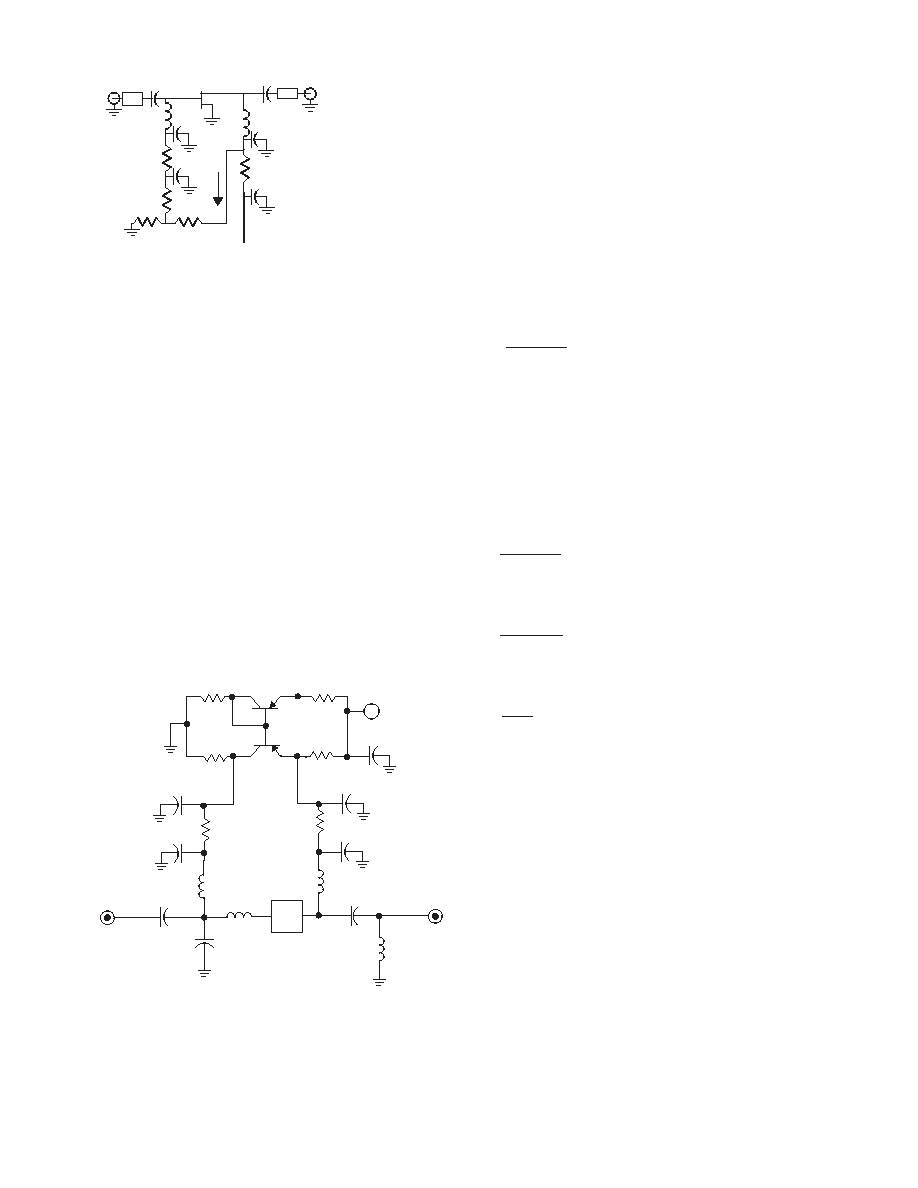
16
Figure 8. Passive Biasing.
Active Bias[2]
Due to very high DC power dissipation and small
package constraints, it is recommended that ATF521P8
use active biasing. The main advantage of an active
biasing scheme is the ability to hold the drain to source
current constant over a wide range of temperature
variations.
A very inexpensive method of accomplishing this
is to use two PNP bipolar transistors arranged in a
current mirror configuration as shown in Figure 9. Due
to resistors R1 and R3, this circuit is not acting as a
true current mirror, but if the voltage drop across R1
and R3 is kept identical then it still displays some of
the more useful characteristics of a current mirror. For
example, transistor Q1 is configured with its base and
collector tied together. This acts as a simple PN junction,
which helps temperature compensate the EmitterBase
junction of Q2.
To calculate the values of R1, R2, R3, and R4 the
following parameters must be know or chosen first:
I
ds is the device draintosource current;
I
R is the Reference current for active bias;
V
dd is the power supply voltage available;
V
ds is the device draintosource voltage;
V
g is the typical gate bias;
V
be1 is the typical BaseEmitter turn on voltage for Q1 &
Q2;
Therefore, resistor R3, which sets the desired device
drain current, is calculated as follows:
R3 = Vdd – Vds
(4)
p
I
ds + IC2
where,
I
C2 is chosen for stability to be 10 times the typical gate
current and also equal to the reference current I
R.
The next three equations are used to calculate the
rest of the biasing resistors for Figure 9. Note that the
voltage drop across R1 must be set equal to the voltage
drop across R3, but with a current of I
R.
R1 = Vdd – Vds
(5)
I
R
R2 sets the bias current through Q1.
R2 = Vds – Vbe1
(6)
p
I
R
R4 sets the gate voltage for ATF521P8.
R4 = Vg
(7)
p
I
C2
Thus, by forcing the emitter voltage (V
E) of transistor
Q1 equal to V
ds, this circuit regulates the drain current
similar to a current mirror. As long as Q2 operates in the
forward active mode, this holds true. In other words, the
CollectorBase junction of Q2 must be kept reversed
biased.
C1
RFin
RFout
L4
L1
L2
L3
R6
R5
R3
R4
C4
C3
C7
C8
C6
C5
Q2
C2
R1
R2
Q1
VE
Vg
Vds
Vdd
2
7
ATF-521P8
2PL
Figure 9. Active Bias Circuit.
INPUT
OUTPUT
Zo
C1
C4
Zo
C5
C6
Vdd
R3
L4
L1
R4
R5
C3
C2
R1
R2
Q1
Ib
相关PDF资料 |
PDF描述 |
|---|---|
| ATF-521P8-BLK | L BAND, Si, N-CHANNEL, RF SMALL SIGNAL, HEMFET, MO-229 |
| ATF-53189-TR1 | C BAND, Si, N-CHANNEL, RF SMALL SIGNAL, HEMFET |
| ATF-53189-BLK | C BAND, Si, N-CHANNEL, RF SMALL SIGNAL, HEMFET |
| ATF-531P8-BLK | C BAND, Si, N-CHANNEL, RF SMALL SIGNAL, HEMFET, MO-229 |
| ATF-531P8-TR1G | C BAND, Si, N-CHANNEL, RF SMALL SIGNAL, HEMFET, MO-229 |
相关代理商/技术参数 |
参数描述 |
|---|---|
| ATF-521P8-TR2 | 功能描述:射频GaAs晶体管 Transistor GaAs High Linearity RoHS:否 制造商:TriQuint Semiconductor 技术类型:pHEMT 频率:500 MHz to 3 GHz 增益:10 dB 噪声系数: 正向跨导 gFS(最大值/最小值):4 S 漏源电压 VDS: 闸/源击穿电压:- 8 V 漏极连续电流:3 A 最大工作温度:+ 150 C 功率耗散:10 W 安装风格: 封装 / 箱体: |
| ATF524S16M | 制造商:n/a 功能描述:Inverter Semiconductor |
| ATF-53189 | 制造商:AGILENT 制造商全称:AGILENT 功能描述:Enhancement Mode Pseudomorphic HEMT in SOT 89 Package |
| ATF-53189-BLK | 功能描述:射频GaAs晶体管 Transistor GaAs High Linearity RoHS:否 制造商:TriQuint Semiconductor 技术类型:pHEMT 频率:500 MHz to 3 GHz 增益:10 dB 噪声系数: 正向跨导 gFS(最大值/最小值):4 S 漏源电压 VDS: 闸/源击穿电压:- 8 V 漏极连续电流:3 A 最大工作温度:+ 150 C 功率耗散:10 W 安装风格: 封装 / 箱体: |
| ATF-53189-TR1 | 功能描述:射频GaAs晶体管 Transistor GaAs High Linearity RoHS:否 制造商:TriQuint Semiconductor 技术类型:pHEMT 频率:500 MHz to 3 GHz 增益:10 dB 噪声系数: 正向跨导 gFS(最大值/最小值):4 S 漏源电压 VDS: 闸/源击穿电压:- 8 V 漏极连续电流:3 A 最大工作温度:+ 150 C 功率耗散:10 W 安装风格: 封装 / 箱体: |
发布紧急采购,3分钟左右您将得到回复。