- 您现在的位置:买卖IC网 > PDF目录11812 > ATMEGA1284P-MUR (Atmel)MCU AVR 128KB FLASH 20MHZ 44VQFN PDF资料下载
参数资料
| 型号: | ATMEGA1284P-MUR |
| 厂商: | Atmel |
| 文件页数: | 132/160页 |
| 文件大小: | 0K |
| 描述: | MCU AVR 128KB FLASH 20MHZ 44VQFN |
| 产品培训模块: | MCU Product Line Introduction megaAVR Introduction |
| 标准包装: | 4,000 |
| 系列: | AVR® ATmega |
| 核心处理器: | AVR |
| 芯体尺寸: | 8-位 |
| 速度: | 20MHz |
| 连通性: | I²C,SPI,UART/USART |
| 外围设备: | 欠压检测/复位,POR,PWM,WDT |
| 输入/输出数: | 32 |
| 程序存储器容量: | 128KB(64K x 16) |
| 程序存储器类型: | 闪存 |
| EEPROM 大小: | 4K x 8 |
| RAM 容量: | 16K x 8 |
| 电压 - 电源 (Vcc/Vdd): | 1.8 V ~ 5.5 V |
| 数据转换器: | A/D 8x10b |
| 振荡器型: | 内部 |
| 工作温度: | -40°C ~ 85°C |
| 封装/外壳: | 44-VFQFN 裸露焊盘 |
| 包装: | 带卷 (TR) |
| 配用: | ATSTK600-ND - DEV KIT FOR AVR/AVR32 |
| 其它名称: | ATMEGA1284P-MUR-ND |
第1页第2页第3页第4页第5页第6页第7页第8页第9页第10页第11页第12页第13页第14页第15页第16页第17页第18页第19页第20页第21页第22页第23页第24页第25页第26页第27页第28页第29页第30页第31页第32页第33页第34页第35页第36页第37页第38页第39页第40页第41页第42页第43页第44页第45页第46页第47页第48页第49页第50页第51页第52页第53页第54页第55页第56页第57页第58页第59页第60页第61页第62页第63页第64页第65页第66页第67页第68页第69页第70页第71页第72页第73页第74页第75页第76页第77页第78页第79页第80页第81页第82页第83页第84页第85页第86页第87页第88页第89页第90页第91页第92页第93页第94页第95页第96页第97页第98页第99页第100页第101页第102页第103页第104页第105页第106页第107页第108页第109页第110页第111页第112页第113页第114页第115页第116页第117页第118页第119页第120页第121页第122页第123页第124页第125页第126页第127页第128页第129页第130页第131页当前第132页第133页第134页第135页第136页第137页第138页第139页第140页第141页第142页第143页第144页第145页第146页第147页第148页第149页第150页第151页第152页第153页第154页第155页第156页第157页第158页第159页第160页
73
8272E–AVR–04/2013
ATmega164A/PA/324A/PA/644A/PA/1284/P
Note that enabling the alternate function of some of the port pins does not affect the use of the
other pins in the port as general digital I/O.
14.2
Ports as General Digital I/O
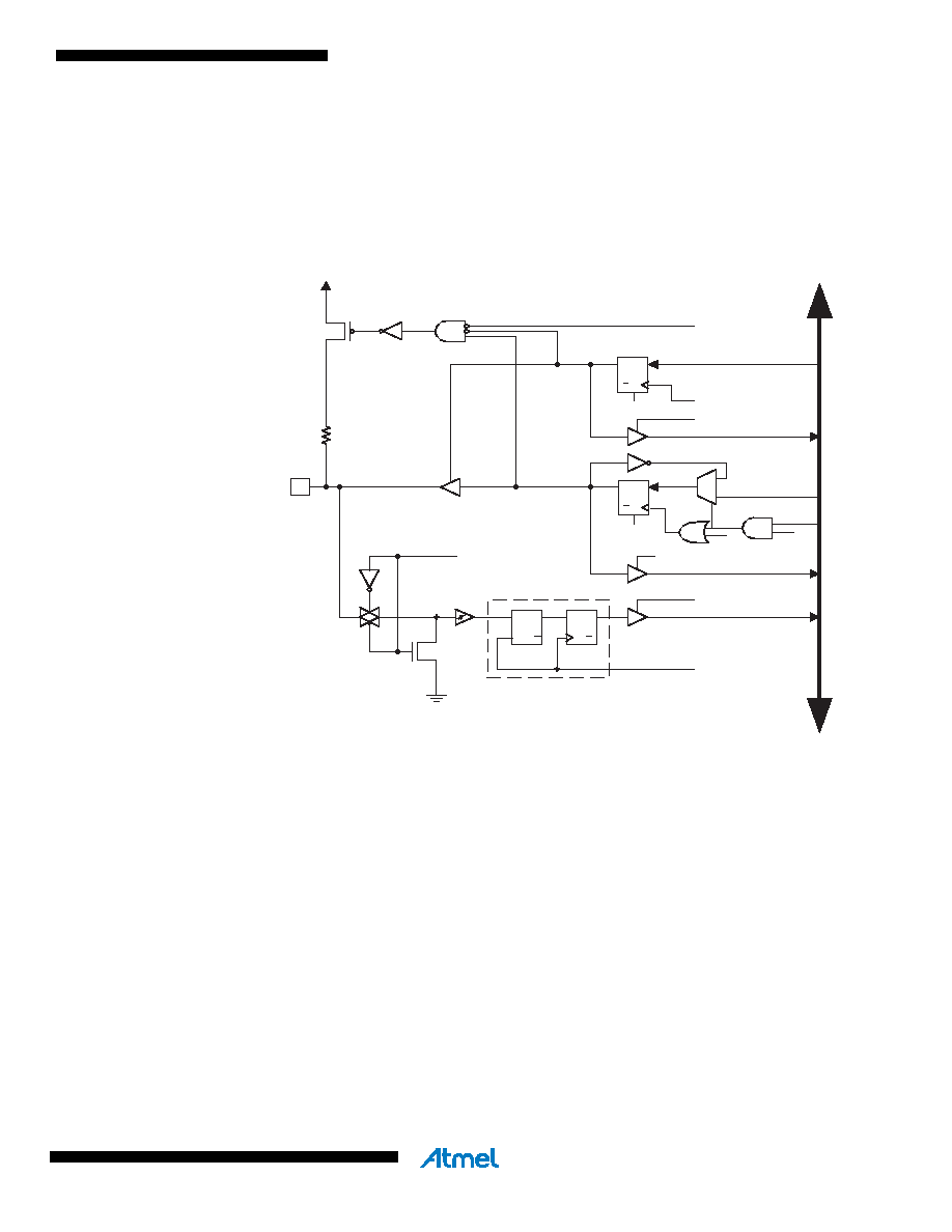
The ports are bi-directional I/O ports with optional internal pull-ups. Figure 14-2 shows a func-
tional description of one I/O-port pin, here generically called Pxn.
Figure 14-2. General digital I/O
(1).
Note:
1. WRx, WPx, WDx, RRx, RPx, and RDx are common to all pins within the same port. clkI/O,
SLEEP, and PUD are common to all ports.
14.2.1
Configuring the Pin
Each port pin consists of three register bits: DDxn, PORTxn, and PINxn. As shown in ”Register
description” on page 91, the DDxn bits are accessed at the DDRx I/O address, the PORTxn bits
at the PORTx I/O address, and the PINxn bits at the PINx I/O address.
The DDxn bit in the DDRx Register selects the direction of this pin. If DDxn is written logic one,
Pxn is configured as an output pin. If DDxn is written logic zero, Pxn is configured as an input
pin.
If PORTxn is written logic one when the pin is configured as an input pin, the pull-up resistor is
activated. To switch the pull-up resistor off, PORTxn has to be written logic zero or the pin has to
be configured as an output pin. The port pins are tri-stated when reset condition becomes active,
even if no clocks are running.
clk
RPx
RRx
RDx
WDx
PUD
SYNCHRONIZER
WDx:
WRITE DDRx
WRx:
WRITE PORTx
RRx:
READ PORTx REGISTER
RPx:
READ PORTx PIN
PUD:
PULLUP DISABLE
clk
I/O:
I/O CLOCK
RDx:
READ DDRx
D
L
Q
RESET
Q
D
Q
D
CLR
PORTxn
Q
D
CLR
DDxn
PINxn
DA
TA
B
U
S
SLEEP
SLEEP:
SLEEP CONTROL
Pxn
I/O
WPx
0
1
WRx
WPx:
WRITE PINx REGISTER
相关PDF资料 |
PDF描述 |
|---|---|
| AT89C51RB2-SLRUM | MCU 8051 16K FLASH 5V 44-PLCC |
| AT89C51RB2-SLRUL | MCU 8051 16K FLASH 3V 44-PLCC |
| MS27484E14B18S | CONN PLUG 18POS STRAIGHT W/SCKT |
| MS27473E12A98PB | CONN PLUG 10POS STRAIGHT W/PINS |
| D38999/20FD19PB | CONN RCPT 19POS WALL MNT W/PINS |
相关代理商/技术参数 |
参数描述 |
|---|---|
| ATMEGA1284P-PU | 功能描述:8位微控制器 -MCU 128KB Flash 20MHz 1.8V-5.5V RoHS:否 制造商:Silicon Labs 核心:8051 处理器系列:C8051F39x 数据总线宽度:8 bit 最大时钟频率:50 MHz 程序存储器大小:16 KB 数据 RAM 大小:1 KB 片上 ADC:Yes 工作电源电压:1.8 V to 3.6 V 工作温度范围:- 40 C to + 105 C 封装 / 箱体:QFN-20 安装风格:SMD/SMT |
| ATMEGA1284PR212-AU | 功能描述:8位微控制器 -MCU ATmega 1284P-AU AT86RF212-ZU RoHS:否 制造商:Silicon Labs 核心:8051 处理器系列:C8051F39x 数据总线宽度:8 bit 最大时钟频率:50 MHz 程序存储器大小:16 KB 数据 RAM 大小:1 KB 片上 ADC:Yes 工作电源电压:1.8 V to 3.6 V 工作温度范围:- 40 C to + 105 C 封装 / 箱体:QFN-20 安装风格:SMD/SMT |
| ATMEGA1284PR212-MU | 功能描述:8位微控制器 -MCU ATmega 1284P-MU AT86RF212-ZU RoHS:否 制造商:Silicon Labs 核心:8051 处理器系列:C8051F39x 数据总线宽度:8 bit 最大时钟频率:50 MHz 程序存储器大小:16 KB 数据 RAM 大小:1 KB 片上 ADC:Yes 工作电源电压:1.8 V to 3.6 V 工作温度范围:- 40 C to + 105 C 封装 / 箱体:QFN-20 安装风格:SMD/SMT |
| ATMEGA1284PR231-AU | 功能描述:8位微控制器 -MCU ATmega 1284P-AU AT86RF231-ZUU RoHS:否 制造商:Silicon Labs 核心:8051 处理器系列:C8051F39x 数据总线宽度:8 bit 最大时钟频率:50 MHz 程序存储器大小:16 KB 数据 RAM 大小:1 KB 片上 ADC:Yes 工作电源电压:1.8 V to 3.6 V 工作温度范围:- 40 C to + 105 C 封装 / 箱体:QFN-20 安装风格:SMD/SMT |
| ATMEGA1284PR231-MU | 功能描述:8位微控制器 -MCU ATmega 1284P-MU AT86RF231-ZU RoHS:否 制造商:Silicon Labs 核心:8051 处理器系列:C8051F39x 数据总线宽度:8 bit 最大时钟频率:50 MHz 程序存储器大小:16 KB 数据 RAM 大小:1 KB 片上 ADC:Yes 工作电源电压:1.8 V to 3.6 V 工作温度范围:- 40 C to + 105 C 封装 / 箱体:QFN-20 安装风格:SMD/SMT |
发布紧急采购,3分钟左右您将得到回复。