参数资料
| 型号: | ATMEGA3250-16AI |
| 厂商: | Atmel |
| 文件页数: | 17/29页 |
| 文件大小: | 0K |
| 描述: | IC AVR MCU 32K 16MHZ 100TQFP |
| 产品培训模块: | megaAVR Introduction |
| 标准包装: | 90 |
| 系列: | AVR® ATmega |
| 核心处理器: | AVR |
| 芯体尺寸: | 8-位 |
| 速度: | 16MHz |
| 连通性: | SPI,UART/USART,USI |
| 外围设备: | 欠压检测/复位,POR,PWM,WDT |
| 输入/输出数: | 69 |
| 程序存储器容量: | 32KB(16K x 16) |
| 程序存储器类型: | 闪存 |
| EEPROM 大小: | 1K x 8 |
| RAM 容量: | 2K x 8 |
| 电压 - 电源 (Vcc/Vdd): | 2.7 V ~ 5.5 V |
| 数据转换器: | A/D 8x10b |
| 振荡器型: | 内部 |
| 工作温度: | -40°C ~ 85°C |
| 封装/外壳: | 100-TQFP |
| 包装: | 托盘 |
| 配用: | ATSTK600-TQFP100-ND - STK600 SOCKET/ADAPTER 100-TQFP ATSTK504-ND - STARTER KIT AVR EXP MOD 100P LCD |
第1页第2页第3页第4页第5页第6页第7页第8页第9页第10页第11页第12页第13页第14页第15页第16页当前第17页第18页第19页第20页第21页第22页第23页第24页第25页第26页第27页第28页第29页
PCA9698
All information provided in this document is subject to legal disclaimers.
NXP B.V. 2010. All rights reserved.
Product data sheet
Rev. 3 — 3 August 2010
24 of 48
NXP Semiconductors
PCA9698
40-bit Fm+ I2C-bus advanced I/O port with RESET, OE and INT
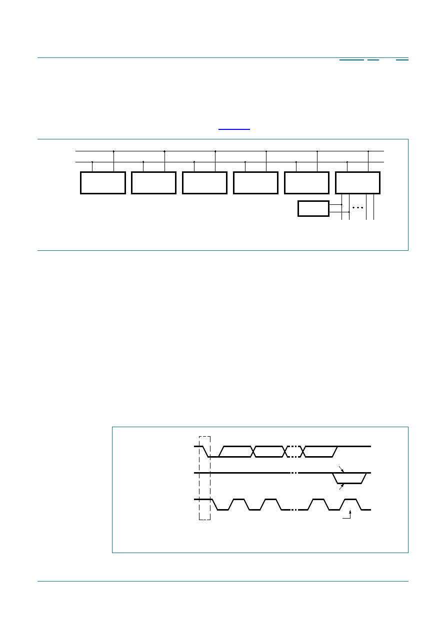
8.2 System configuration
A device generating a message is a ‘transmitter’; a device receiving is the ‘receiver’. The
device that controls the message is the ‘master’ and the devices which are controlled by
the master are the ‘slaves’ (see Figure 13).
8.3 Acknowledge
The number of data bytes transferred between the START and the STOP conditions from
transmitter to receiver is not limited. Each byte of eight bits is followed by one
acknowledge bit. The acknowledge bit is a HIGH level put on the bus by the transmitter,
whereas the master generates an extra acknowledge related clock pulse.
A slave receiver which is addressed must generate an acknowledge after the reception of
each byte. Also a master must generate an acknowledge after the reception of each byte
that has been clocked out of the slave transmitter. The device that acknowledges has to
pull down the SDA line during the acknowledge clock pulse, so that the SDA line is stable
LOW during the HIGH period of the acknowledge related clock pulse; set-up and hold
times must be taken into account.
A master receiver must signal an end of data to the transmitter by not generating an
acknowledge on the last byte that has been clocked out of the slave. In this event, the
transmitter must leave the data line HIGH to enable the master to generate a STOP
condition.
Fig 13. System configuration
002aaa966
MASTER
TRANSMITTER/
RECEIVER
SLAVE
RECEIVER
SLAVE
TRANSMITTER/
RECEIVER
MASTER
TRANSMITTER
MASTER
TRANSMITTER/
RECEIVER
SDA
SCL
I2C-BUS
MULTIPLEXER
SLAVE
Fig 14. Acknowledgement on the I2C-bus
002aaa987
S
START
condition
9
8
2
1
clock pulse for
acknowledgement
not acknowledge
acknowledge
data output
by transmitter
data output
by receiver
SCL from master
相关PDF资料 |
PDF描述 |
|---|---|
| PIC18F4420-I/ML | IC MCU FLASH 8KX16 44QFN |
| DSPIC30F3014-20I/PT | IC DSPIC MCU/DSP 24K 44TQFP |
| ATMEGA325V-8MI | IC AVR MCU 32K 8MHZ 64-QFN |
| PIC16F74-I/P | IC MCU FLASH 4KX14 A/D 40DIP |
| ATMEGA165-16AI | IC AVR MCU 16K 16MHZ 64TQFP |
相关代理商/技术参数 |
参数描述 |
|---|---|
| ATMEGA3250-16AJ | 制造商:ATMEL 制造商全称:ATMEL Corporation 功能描述:8-bit Microcontroller with In-System Programmable Flash |
| ATmega3250-16AU | 功能描述:8位微控制器 -MCU AVR 32K FLASH 1K EE 2K SRAM ADC 5V 5V RoHS:否 制造商:Silicon Labs 核心:8051 处理器系列:C8051F39x 数据总线宽度:8 bit 最大时钟频率:50 MHz 程序存储器大小:16 KB 数据 RAM 大小:1 KB 片上 ADC:Yes 工作电源电压:1.8 V to 3.6 V 工作温度范围:- 40 C to + 105 C 封装 / 箱体:QFN-20 安装风格:SMD/SMT |
| ATMEGA3250-16AUR | 功能描述:8位微控制器 -MCU AVR 32K FLSH 1K EE2K SRAM ADC 5V-16MHZ 5V RoHS:否 制造商:Silicon Labs 核心:8051 处理器系列:C8051F39x 数据总线宽度:8 bit 最大时钟频率:50 MHz 程序存储器大小:16 KB 数据 RAM 大小:1 KB 片上 ADC:Yes 工作电源电压:1.8 V to 3.6 V 工作温度范围:- 40 C to + 105 C 封装 / 箱体:QFN-20 安装风格:SMD/SMT |
| ATMEGA3250A | 制造商:ATMEL 制造商全称:ATMEL Corporation 功能描述:8-bit Microcontroller with 16/32/64K Bytes In-System Programmable Flash |
| ATMEGA3250A-AN | 功能描述:8位微控制器 -MCU AVR 32K FL 2K SRAM 1KB EE 20 MHZ GRN RoHS:否 制造商:Silicon Labs 核心:8051 处理器系列:C8051F39x 数据总线宽度:8 bit 最大时钟频率:50 MHz 程序存储器大小:16 KB 数据 RAM 大小:1 KB 片上 ADC:Yes 工作电源电压:1.8 V to 3.6 V 工作温度范围:- 40 C to + 105 C 封装 / 箱体:QFN-20 安装风格:SMD/SMT |
发布紧急采购,3分钟左右您将得到回复。