参数资料
| 型号: | ATMEGA3250-16AI |
| 厂商: | Atmel |
| 文件页数: | 20/29页 |
| 文件大小: | 0K |
| 描述: | IC AVR MCU 32K 16MHZ 100TQFP |
| 产品培训模块: | megaAVR Introduction |
| 标准包装: | 90 |
| 系列: | AVR® ATmega |
| 核心处理器: | AVR |
| 芯体尺寸: | 8-位 |
| 速度: | 16MHz |
| 连通性: | SPI,UART/USART,USI |
| 外围设备: | 欠压检测/复位,POR,PWM,WDT |
| 输入/输出数: | 69 |
| 程序存储器容量: | 32KB(16K x 16) |
| 程序存储器类型: | 闪存 |
| EEPROM 大小: | 1K x 8 |
| RAM 容量: | 2K x 8 |
| 电压 - 电源 (Vcc/Vdd): | 2.7 V ~ 5.5 V |
| 数据转换器: | A/D 8x10b |
| 振荡器型: | 内部 |
| 工作温度: | -40°C ~ 85°C |
| 封装/外壳: | 100-TQFP |
| 包装: | 托盘 |
| 配用: | ATSTK600-TQFP100-ND - STK600 SOCKET/ADAPTER 100-TQFP ATSTK504-ND - STARTER KIT AVR EXP MOD 100P LCD |
第1页第2页第3页第4页第5页第6页第7页第8页第9页第10页第11页第12页第13页第14页第15页第16页第17页第18页第19页当前第20页第21页第22页第23页第24页第25页第26页第27页第28页第29页
PCA9698
All information provided in this document is subject to legal disclaimers.
NXP B.V. 2010. All rights reserved.
Product data sheet
Rev. 3 — 3 August 2010
27 of 48
NXP Semiconductors
PCA9698
40-bit Fm+ I2C-bus advanced I/O port with RESET, OE and INT
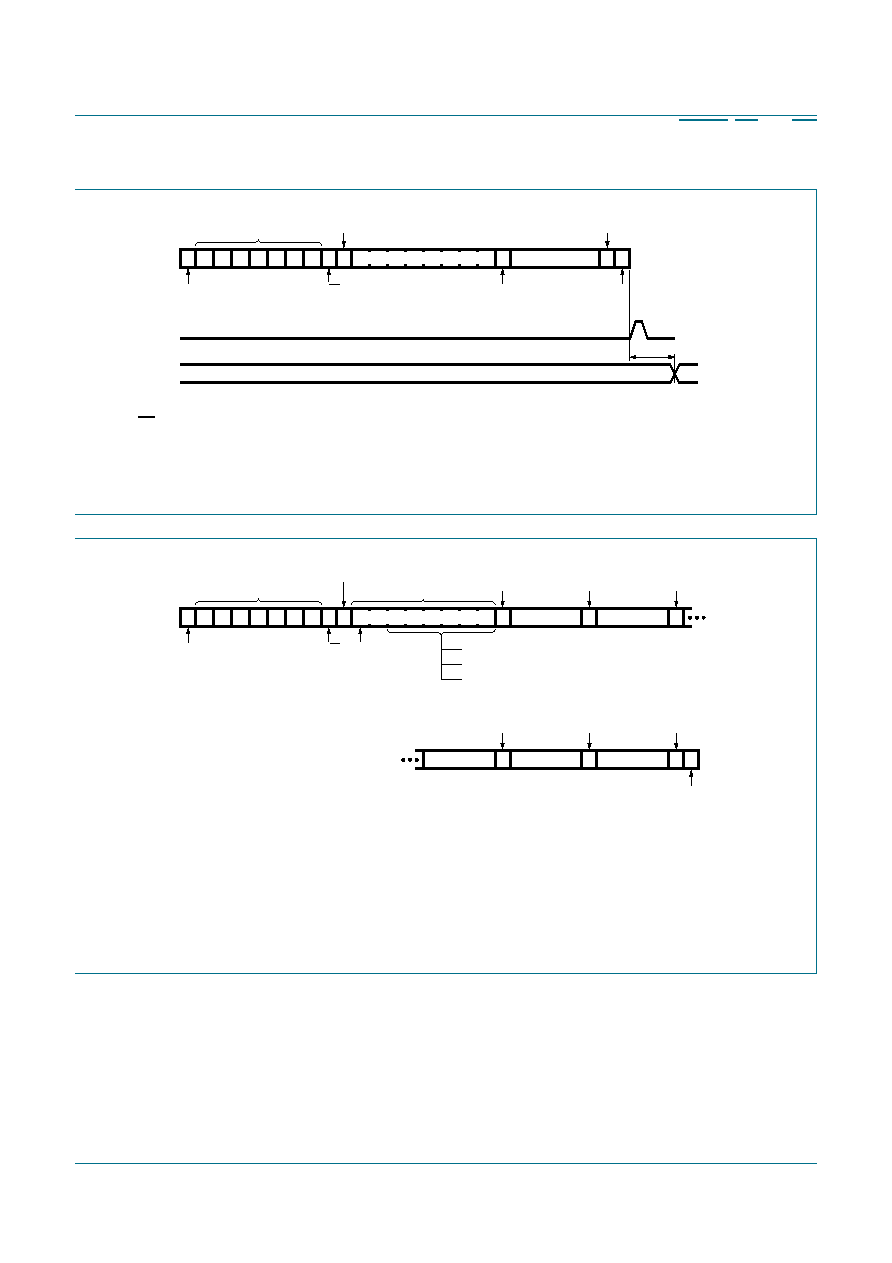
OE is LOW (with OEPOL = 0) or HIGH (with OEPOL = 1) to observe a change in the outputs.
OCH = 0. When OCH = 1, the change in the port happens at the acknowledge phase.
Two, three, or four adjacent banks can be programmed by using the Auto-Increment feature (AI = 1) and change at the
corresponding output port becomes effective at the STOP command when OCH = 0, or at each acknowledge when OCH = 1.
Fig 16. Write to a specific output port
002aab945
S A6 A5 A4 A3 A2 A1 A0 0 A
slave address
R/W
START condition
A
acknowledge
from slave
DATA BANK X
P
STOP
condition
A
SDA
tv(Q)
write to port
data out from port
data X valid
AI
0001 D2 D1 D0
acknowledge
from slave
acknowledge
from slave
bank X
determined by
D2, D1, D0
The programing becomes effective at the Acknowledge.
Less than 5 bytes can be programmed by using the same scheme. ‘D5 D4 D3 D2 D1 D0’ refers to the first register to be
programmed.
If more than 5 bytes are written, previous data are overwritten (the sixth configuration register will roll over to the first addressed
configuration register, the sixth Polarity Inversion register will roll over to the first addressed Polarity Inversion register, the sixth
Mask interrupt register will roll over to the first addressed Mask interrupt register.
Fig 17. Write to the I/O Configuration, Polarity Inversion, or Mask interrupt registers (5 banks)
002aab946
S A6 A5 A4 A3 A2 A1 A0 0 A
slave address
R/W
START condition
command register
AI = 1
A
acknowledge
from slave
DATA BANK 0 A
acknowledge
from slave
DATA BANK 1
acknowledge
from slave
A
acknowledge
from slave
DATA BANK 2 A
acknowledge
from slave
DATA BANK 3 A
acknowledge
from slave
DATA BANK 4
P
STOP
condition
A
SDA
1
0 D5 D4 D3 D2 D1 D0
01 0000 for Polarity Inversion register programming bank 0
01 1000 for Configuration register programming bank 0
10 0000 for Mask interrupt register programming bank 0
acknowledge
from slave
相关PDF资料 |
PDF描述 |
|---|---|
| PIC18F4420-I/ML | IC MCU FLASH 8KX16 44QFN |
| DSPIC30F3014-20I/PT | IC DSPIC MCU/DSP 24K 44TQFP |
| ATMEGA325V-8MI | IC AVR MCU 32K 8MHZ 64-QFN |
| PIC16F74-I/P | IC MCU FLASH 4KX14 A/D 40DIP |
| ATMEGA165-16AI | IC AVR MCU 16K 16MHZ 64TQFP |
相关代理商/技术参数 |
参数描述 |
|---|---|
| ATMEGA3250-16AJ | 制造商:ATMEL 制造商全称:ATMEL Corporation 功能描述:8-bit Microcontroller with In-System Programmable Flash |
| ATmega3250-16AU | 功能描述:8位微控制器 -MCU AVR 32K FLASH 1K EE 2K SRAM ADC 5V 5V RoHS:否 制造商:Silicon Labs 核心:8051 处理器系列:C8051F39x 数据总线宽度:8 bit 最大时钟频率:50 MHz 程序存储器大小:16 KB 数据 RAM 大小:1 KB 片上 ADC:Yes 工作电源电压:1.8 V to 3.6 V 工作温度范围:- 40 C to + 105 C 封装 / 箱体:QFN-20 安装风格:SMD/SMT |
| ATMEGA3250-16AUR | 功能描述:8位微控制器 -MCU AVR 32K FLSH 1K EE2K SRAM ADC 5V-16MHZ 5V RoHS:否 制造商:Silicon Labs 核心:8051 处理器系列:C8051F39x 数据总线宽度:8 bit 最大时钟频率:50 MHz 程序存储器大小:16 KB 数据 RAM 大小:1 KB 片上 ADC:Yes 工作电源电压:1.8 V to 3.6 V 工作温度范围:- 40 C to + 105 C 封装 / 箱体:QFN-20 安装风格:SMD/SMT |
| ATMEGA3250A | 制造商:ATMEL 制造商全称:ATMEL Corporation 功能描述:8-bit Microcontroller with 16/32/64K Bytes In-System Programmable Flash |
| ATMEGA3250A-AN | 功能描述:8位微控制器 -MCU AVR 32K FL 2K SRAM 1KB EE 20 MHZ GRN RoHS:否 制造商:Silicon Labs 核心:8051 处理器系列:C8051F39x 数据总线宽度:8 bit 最大时钟频率:50 MHz 程序存储器大小:16 KB 数据 RAM 大小:1 KB 片上 ADC:Yes 工作电源电压:1.8 V to 3.6 V 工作温度范围:- 40 C to + 105 C 封装 / 箱体:QFN-20 安装风格:SMD/SMT |
发布紧急采购,3分钟左右您将得到回复。