- 您现在的位置:买卖IC网 > PDF目录12028 > ATMEGA6450-16AU (Atmel)IC AVR MCU FLASH 64K 100TQFP PDF资料下载
参数资料
| 型号: | ATMEGA6450-16AU |
| 厂商: | Atmel |
| 文件页数: | 32/85页 |
| 文件大小: | 0K |
| 描述: | IC AVR MCU FLASH 64K 100TQFP |
| 产品培训模块: | MCU Product Line Introduction megaAVR Introduction |
| 标准包装: | 90 |
| 系列: | AVR® ATmega |
| 核心处理器: | AVR |
| 芯体尺寸: | 8-位 |
| 速度: | 16MHz |
| 连通性: | SPI,UART/USART,USI |
| 外围设备: | 欠压检测/复位,POR,PWM,WDT |
| 输入/输出数: | 68 |
| 程序存储器容量: | 64KB(32K x 16) |
| 程序存储器类型: | 闪存 |
| EEPROM 大小: | 2K x 8 |
| RAM 容量: | 4K x 8 |
| 电压 - 电源 (Vcc/Vdd): | 2.7 V ~ 5.5 V |
| 数据转换器: | A/D 8x10b |
| 振荡器型: | 内部 |
| 工作温度: | -40°C ~ 85°C |
| 封装/外壳: | 100-TQFP |
| 包装: | 托盘 |
| 产品目录页面: | 614 (CN2011-ZH PDF) |
| 配用: | ATSTK600-RC18-ND - STK600 ROUTING CARD AVR ATSTK600-TQFP100-ND - STK600 SOCKET/ADAPTER 100-TQFP ATAVRISP2-ND - PROGRAMMER AVR IN SYSTEM ATSTK504-ND - STARTER KIT AVR EXP MOD 100P LCD |
第1页第2页第3页第4页第5页第6页第7页第8页第9页第10页第11页第12页第13页第14页第15页第16页第17页第18页第19页第20页第21页第22页第23页第24页第25页第26页第27页第28页第29页第30页第31页当前第32页第33页第34页第35页第36页第37页第38页第39页第40页第41页第42页第43页第44页第45页第46页第47页第48页第49页第50页第51页第52页第53页第54页第55页第56页第57页第58页第59页第60页第61页第62页第63页第64页第65页第66页第67页第68页第69页第70页第71页第72页第73页第74页第75页第76页第77页第78页第79页第80页第81页第82页第83页第84页第85页
2010-2011 Microchip Technology Inc.
Preliminary
DS41419C-page 255
PIC16(L)F1824/1828
25.3
I2C
Mode Overview
The Inter-Integrated Circuit Bus (IC) is a multi-master
serial data communication bus. Devices communicate
in a master/slave environment where the master
devices initiate the communication. A Slave device is
controlled through addressing.
The I2C bus specifies two signal connections:
Serial Clock (SCL)
Serial Data (SDA)
Figure 25-2 and Figure 25-3 shows the block diagram
of the MSSP1 module when operating in I2C Mode.
Both the SCL and SDA connections are bidirectional
open-drain lines, each requiring pull-up resistors for the
supply voltage. Pulling the line to ground is considered
a logical zero and letting the line float is considered a
logical one.
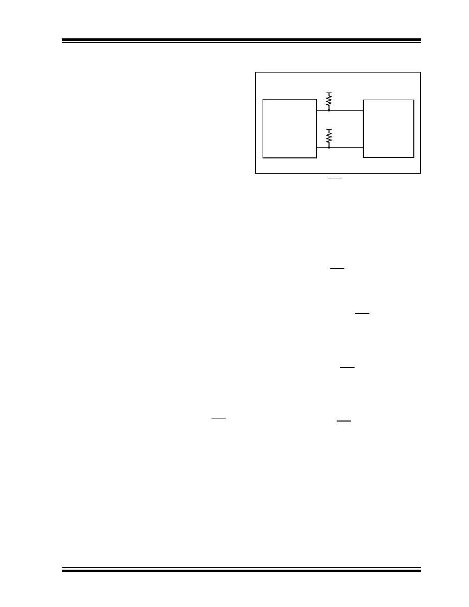
Figure 25-11 shows a typical connection between two
processors configured as master and slave devices.
The I2C bus can operate with one or more master
devices and one or more slave devices.
There are four potential modes of operation for a given
device:
Master Transmit mode
(master is transmitting data to a slave)
Master Receive mode
(master is receiving data from a slave)
Slave Transmit mode
(slave is transmitting data to a master)
Slave Receive mode
(slave is receiving data from the master)
To begin communication, a master device starts out in
Master Transmit mode. The master device sends out a
Start bit followed by the address byte of the slave it
intends to communicate with. This is followed by a sin-
gle Read/Write bit, which determines whether the mas-
ter intends to transmit to or receive data from the slave
device.
If the requested slave exists on the bus, it will respond
with an Acknowledge bit, otherwise known as an ACK.
The master then continues in either Transmit mode or
Receive mode and the slave continues in the comple-
ment, either in Receive mode or Transmit mode,
respectively.
A Start bit is indicated by a high-to-low transition of the
SDA line while the SCL line is held high. Address and
data bytes are sent out, Most Significant bit (MSb) first.
The Read/Write bit is sent out as a logical one when the
master intends to read data from the slave, and is sent
out as a logical zero when it intends to write data to the
slave.
FIGURE 25-11:
I2C MASTER/
SLAVE CONNECTION
The Acknowledge bit (ACK) is an active-low signal,
which holds the SDA line low to indicate to the transmit-
ter that the slave device has received the transmitted
data and is ready to receive more.
The transition of a data bit is always performed while
the SCL line is held low. Transitions that occur while the
SCL line is held high are used to indicate Start and Stop
bits.
If the master intends to write to the slave, then it repeat-
edly sends out a byte of data, with the slave responding
after each byte with an ACK bit. In this example, the
master device is in Master Transmit mode and the
slave is in Slave Receive mode.
If the master intends to read from the slave, then it
repeatedly receives a byte of data from the slave, and
responds after each byte with an ACK bit. In this exam-
ple, the master device is in Master Receive mode and
the slave is Slave Transmit mode.
On the last byte of data communicated, the master
device may end the transmission by sending a Stop bit.
If the master device is in Receive mode, it sends the
Stop bit in place of the last ACK bit. A Stop bit is indi-
cated by a low-to-high transition of the SDA line while
the SCL line is held high.
In some cases, the master may want to maintain con-
trol of the bus and re-initiate another transmission. If
so, the master device may send another Start bit in
place of the Stop bit or last ACK bit when it is in receive
mode.
The I2C bus specifies three message protocols;
Single message where a master writes data to a
slave.
Single message where a master reads data from
a slave.
Combined message where a master initiates a
minimum of two writes, or two reads, or a
combination of writes and reads, to one or more
slaves.
Master
SCL
SDA
SCL
SDA
Slave
VDD
相关PDF资料 |
PDF描述 |
|---|---|
| AT89C51ED2-RLTUM | IC 8051 MCU FLASH 64K 44VQFP |
| AT89C51ED2-SLSUM | IC 8051 MCU FLASH 64K 44PLCC |
| VJ2225A561KBBAT4X | CAP CER 560PF 100V 10% NP0 2225 |
| VI-B23-IY-F4 | CONVERTER MOD DC/DC 24V 50W |
| VI-J1Y-IX-F3 | CONVERTER MOD DC/DC 3.3V 49.5W |
相关代理商/技术参数 |
参数描述 |
|---|---|
| ATMEGA6450-16AUR | 功能描述:8位微控制器 -MCU AVR 64KB FLSH 2KB EE 4KB SRAM-16MHz, 5V RoHS:否 制造商:Silicon Labs 核心:8051 处理器系列:C8051F39x 数据总线宽度:8 bit 最大时钟频率:50 MHz 程序存储器大小:16 KB 数据 RAM 大小:1 KB 片上 ADC:Yes 工作电源电压:1.8 V to 3.6 V 工作温度范围:- 40 C to + 105 C 封装 / 箱体:QFN-20 安装风格:SMD/SMT |
| ATMEGA6450A-AU | 功能描述:8位微控制器 -MCU AVR 64KB FLSH 2KB EE 4KB SRAM-20MHz, IND RoHS:否 制造商:Silicon Labs 核心:8051 处理器系列:C8051F39x 数据总线宽度:8 bit 最大时钟频率:50 MHz 程序存储器大小:16 KB 数据 RAM 大小:1 KB 片上 ADC:Yes 工作电源电压:1.8 V to 3.6 V 工作温度范围:- 40 C to + 105 C 封装 / 箱体:QFN-20 安装风格:SMD/SMT |
| ATMEGA6450A-AUR | 功能描述:8位微控制器 -MCU AVR 64KB FLSH 2KB EE 4KB SRAM-20MHz, IND RoHS:否 制造商:Silicon Labs 核心:8051 处理器系列:C8051F39x 数据总线宽度:8 bit 最大时钟频率:50 MHz 程序存储器大小:16 KB 数据 RAM 大小:1 KB 片上 ADC:Yes 工作电源电压:1.8 V to 3.6 V 工作温度范围:- 40 C to + 105 C 封装 / 箱体:QFN-20 安装风格:SMD/SMT |
| ATMEGA6450P-AU | 功能描述:8位微控制器 -MCU AVR 64KB FLSH 2KB EE 4KB SRAM-16MHz, IND RoHS:否 制造商:Silicon Labs 核心:8051 处理器系列:C8051F39x 数据总线宽度:8 bit 最大时钟频率:50 MHz 程序存储器大小:16 KB 数据 RAM 大小:1 KB 片上 ADC:Yes 工作电源电压:1.8 V to 3.6 V 工作温度范围:- 40 C to + 105 C 封装 / 箱体:QFN-20 安装风格:SMD/SMT |
| ATMEGA6450P-AUR | 功能描述:8位微控制器 -MCU AVR 64KB FLSH 2KB EE 4KB SRAM-16MHz, IND RoHS:否 制造商:Silicon Labs 核心:8051 处理器系列:C8051F39x 数据总线宽度:8 bit 最大时钟频率:50 MHz 程序存储器大小:16 KB 数据 RAM 大小:1 KB 片上 ADC:Yes 工作电源电压:1.8 V to 3.6 V 工作温度范围:- 40 C to + 105 C 封装 / 箱体:QFN-20 安装风格:SMD/SMT |
发布紧急采购,3分钟左右您将得到回复。