参数资料
| 型号: | B048F240T30 |
| 厂商: | Vicor Corporation |
| 文件页数: | 6/12页 |
| 文件大小: | 0K |
| 描述: | CONVERTER BUS 24V OUT 300W SMD |
| 应用说明: | Factorized Power Architecture and V-I Chips |
| 产品培训模块: | VI Chip Bus Converter Modules |
| 标准包装: | 1 |
| 系列: | V-I Chip™, BCM™ |
| 类型: | 总线转换器模块 |
| 输出数: | 1 |
| 电压 - 输入(最小): | 38V |
| 电压 - 输入(最大): | 53V |
| 输出电压: | 24V |
| 电流 - 输出(最大): | 12.5A |
| 电源(瓦) - 制造商系列: | 300W |
| 电压 - 隔离: | 2.25kV(2250V) |
| 应用: | 商用 |
| 特点: | 具有远程开/关功能和 UVLO |
| 安装类型: | 表面贴装 |
| 封装/外壳: | 模块 |
| 尺寸/尺寸: | 1.28" L x 0.87" W x 0.26" H(32.5mm x 22.0mm x 6.7mm) |
| 包装: | 托盘 |
| 工作温度: | -40°C ~ 125°C |
| 效率: | 95.8% |
| 电源(瓦特)- 最大: | 300W |
| 重量: | 0.033 磅(14.97g) |
| 其它名称: | 1102-1002 |
�� �
�
�Not� Recommended� for� New� Designs� -� Replaced� by� BCM48Bx240y300A00�
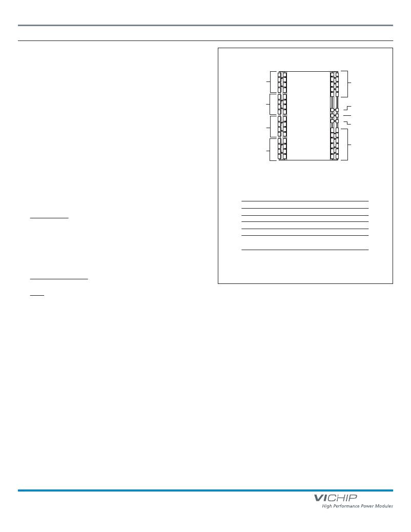
�Pin� /� Control� Functions�
�+In� /� -In� –� DC� Voltage� Input� Ports�
�The� VI� Chip� module� input� voltage� range� should� not� be� exceeded.� An�
�B048F240T30�
�internal� undervoltage� /overvoltage� lockout� function� prevents� operation�
�outside� of� the� normal� operating� input� range.� The� BCM� ?� bus� converter�
�A�
�4�
�3�
�2�
�1�
�A�
�turns� on� within� an� input� voltage� window� bounded� by� the� “Input�
�undervoltage� turn� on”� and� “Input� overvoltage� turn� off”� levels,� as�
�specified.� The� module� may� be� protected� against� accidental� application�
�of� a� reverse� input� voltage� by� the� addition� of� a� rectifier� in� series� with� the�
�positive� input,� or� a� reverse� rectifier� in� shunt� with� the� positive� input�
�located� on� the� load� side� of� the� input� fuse.�
�The� connection� of� the� module� to� its� power� source� should� be�
�implemented� with� minimal� distribution� inductance.� If� the� interconnect�
�inductance� exceeds� 100� nH,� the� input� should� be� bypassed� with� a� RC�
�damper� to� retain� low� source� impedance� and� stable� operation.� With� an�
�interconnect� inductance� of� 200� nH,� the� RC� damper� may� be� 47� μF� in�
�+Out�
�-Out�
�+Out�
�-Out�
�B�
�C�
�D�
�E�
�F�
�G�
�H�
�J�
�K�
�L�
�M�
�N�
�P�
�R�
�T�
�B�
�C�
�D�
�E�
�H�
�J�
�K�
�L�
�M�
�N�
�P�
�R�
�T�
�+In�
�TM�
�RSV�
�PC�
�-In�
�series� with� 0.3� Ω� .� A� single� electrolytic� or� equivalent� low-Q� capacitor� may�
�be� used� in� place� of� the� series� RC� bypass.�
�Bottom� View�
�PC� –� Primary� Control�
�The� Primary� Control� port� is� a� multifunction� node� that� provides� the�
�following� functions:�
�Enable / Disable� –� If� the� PC� port� is� left� floating,� the� BCM� module�
�output� is� enabled.� Once� this� port� is� pulled� lower� than� 2.4� Vdc� with�
�respect� to� –In,� the� output� is� disabled.� This� action� can� be� realized� by�
�employing� a� relay,� opto-coupler,� or� open� collector� transistor.� Refer�
�to� Figures� 1-3,� 12� and� 13� for� the� typical� enable� /disable�
�characteristics.� This� port� should� not� be� toggled� at� a� rate� higher�
�than� 1� Hz.� The� PC� port� should� also� not� be� driven� by� or� pulled� up� to�
�an� external� voltage� source.�
�Primary Auxiliary Supply� –� The� PC� port� can� source� up� to� 2.4� mA� at�
�5.0� Vdc.� The� PC� port� should� never� be� used� to� sink� current.�
�Signal�
�Name�
�+In�
�–In�
�TM�
�RSV�
�PC�
�+Out�
�–Out�
�Designation�
�A1-E1,� A2-E2�
�L1-T1,� L2-T2�
�H1,� H2�
�J1,� J2�
�K1,� K2�
�A3-D3,� A4-D4,�
�J3-M3,� J4-M4�
�E3-H3,� E4-H4,�
�N3-T3,� N4-T4�
�Alarm� –� The� module� contains� circuitry� that� monitors� output�
�overload,� input� overvoltage� or� undervoltage,� and� internal� junction�
�temperatures.� In� response� to� an� abnormal� condition� in� any� of� the�
�monitored� parameters,� the� PC� port� will� toggle.� Refer� to� Figure� 13�
�for� PC� alarm� characteristics.�
�TM� and� RSV� –� Reserved� for� factory� use.�
�+Out� /� -Out� –� DC� Voltage� Output� Ports�
�Two� sets� of� contacts� are� provided� for� the� +Out� port.� They� must� be�
�connected� in� parallel� with� low� interconnect� resistance.� Similarly,� two�
�sets� of� contacts� are� provided� for� the� –Out� port.� They� must� be�
�connected� in� parallel� with� low� interconnect� resistance.� Within� the�
�specified� operating� range,� the� average� output� voltage� is� defined� by� the�
�Level� 1� DC� behavioral� model� of� Figure� 21.� The� current� source� capability�
�of� the� module� is� rated� in� the� specifications� section� of� this� document.�
�The� low� output� impedance� of� the� module� reduces� or� eliminates� the�
�need� for� limited� life� aluminum� electrolytic� or� tantalum� capacitors� at� the�
�input� of� POL� converters.�
�Total� load� capacitance� at� the� output� of� the� modules� should� not� exceed�
�the� specified� maximum.� Owing� to� the� wide� bandwidth� and� low� output�
�impedance� of� the� module,� low� frequency� bypass� capacitance� and�
�significant� energy� storage� may� be� more� densely� and� efficiently� provided�
�by� adding� capacitance� at� the� input� of� the� BCM� module.�
�Figure� 14� —� BCM� ?� bus� converter� pin� configuration�
�BCM� ?� Bus� Converter�
�Page� 6� of� 12�
�Rev� 2.8�
�01/2014�
�vicorpower.com�
�800� 927.9474�
�相关PDF资料 |
PDF描述 |
|---|---|
| MS27468T21B11A | CONN HSG RCPT 11POS JAMNUT PINS |
| VE-24D-MV-F2 | CONVERTER MOD DC/DC 85V 150W |
| M83723/91W2212NLC | CONN HSG PLUG 12POS STRGHT SCKT |
| VE-24D-MV-F1 | CONVERTER MOD DC/DC 85V 150W |
| MS3456W16-10B | CONN HSG PLUG 3POS STRGHT SCKT |
相关代理商/技术参数 |
参数描述 |
|---|---|
| B048F240T30_12 | 制造商:VICOR 制造商全称:Vicor Corporation 功能描述:Bus Converter |
| B048F240T30A | 功能描述:BCM BUS CONVERTER 24V 300W 制造商:vicor corporation 系列:VI Chip? BCM? 包装:散装 零件状态:有效 类型:总线转换器模块 输出数:1 电压 - 输入(最小值):38V 电压 - 输入(最大值):55V 电压 - 输出 1:24V 电压 - 输出 2:- 电压 - 输出 3:- 电流 - 输出(最大值):12.5A 功率(W) - 制造系列:300W 电压 - 隔离:2.25kV(2250V) 应用:ITE(商业) 特性:远程开/关,OCP,OTP,OVP,SCP,UVLO 安装类型:表面贴装 封装/外壳:模块 大小/尺寸:1.28" 长 x 0.87" 宽 x 0.26" 高(32.5mm x 22.0mm x 6.7mm) 工作温度:-40°C ~ 125°C 效率:95.5% 功率(W) - 最大值:300W 标准包装:1 |
| B048F240T30-EB | 功能描述:EVAL BOARD 24V OUT 300W SMD RoHS:是 类别:编程器,开发系统 >> 评估板 - DC/DC 与 AC/DC(离线)SMPS 系列:V-I Chip™, BCM™ 产品培训模块:Obsolescence Mitigation Program 标准包装:1 系列:True Shutdown™ 主要目的:DC/DC,步升 输出及类型:1,非隔离 功率 - 输出:- 输出电压:- 电流 - 输出:1A 输入电压:2.5 V ~ 5.5 V 稳压器拓扑结构:升压 频率 - 开关:3MHz 板类型:完全填充 已供物品:板 已用 IC / 零件:MAX8969 |
| B048F320M30 | 制造商:VICOR 制造商全称:Vicor Corporation 功能描述:BCM Bus Converter |
| B048F320M30A | 功能描述:BCM BUS CONVERTER 32V 300W 制造商:vicor corporation 系列:VI Chip? BCM? 包装:散装 零件状态:有效 类型:总线转换器模块 输出数:1 电压 - 输入(最小值):38V 电压 - 输入(最大值):55V 电压 - 输出 1:32V 电压 - 输出 2:- 电压 - 输出 3:- 电流 - 输出(最大值):9A 功率(W) - 制造系列:300W 电压 - 隔离:2.25kV(2250V) 应用:ITE(商业) 特性:远程开/关,OCP,OTP,OVP,SCP,UVLO 安装类型:表面贴装 封装/外壳:模块 大小/尺寸:1.28" 长 x 0.87" 宽 x 0.26" 高(32.5mm x 22.0mm x 6.7mm) 工作温度:-55°C ~ 125°C 效率:96.2% 功率(W) - 最大值:300W 标准包装:1 |
发布紧急采购,3分钟左右您将得到回复。