参数资料
| 型号: | BR24S08FVT-WE2 |
| 厂商: | Rohm Semiconductor |
| 文件页数: | 9/41页 |
| 文件大小: | 0K |
| 描述: | IC EEPROM 8KBIT 400KHZ 8TSSOP |
| 标准包装: | 1 |
| 格式 - 存储器: | EEPROMs - 串行 |
| 存储器类型: | EEPROM |
| 存储容量: | 8K (1K x 8) |
| 速度: | 400kHz |
| 接口: | I²C,2 线串口 |
| 电源电压: | 1.7 V ~ 5.5 V |
| 工作温度: | -40°C ~ 85°C |
| 封装/外壳: | 8-TSSOP(0.173",4.40mm 宽) |
| 供应商设备封装: | 8-TSSOP-B |
| 包装: | 标准包装 |
| 产品目录页面: | 1379 (CN2011-ZH PDF) |
| 其它名称: | BR24S08FVT-WE2DKR |
第1页第2页第3页第4页第5页第6页第7页第8页当前第9页第10页第11页第12页第13页第14页第15页第16页第17页第18页第19页第20页第21页第22页第23页第24页第25页第26页第27页第28页第29页第30页第31页第32页第33页第34页第35页第36页第37页第38页第39页第40页第41页
�� �
�
�BR24L� □□� -W� Series,BR24S� □□□� -W� Series�
�Technical� Note�
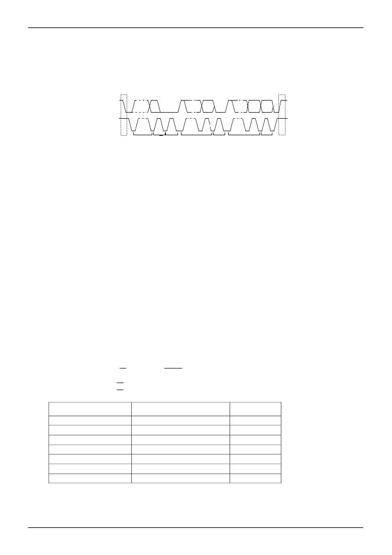
�I� C� BUS� data� communication�
�I� C� BUS� data� communication� starts� by� start� condition� input,� and� ends� by� stop� condition� input.� Data� is� always� 8bit� long,�
�and� acknowledge� is� always� required� after� each� byte.� I� C� BUS� carries� out� data� transmission� with� plural� devices�
�●� I� 2� C� BUS� communication�
�2�
�2�
�2�
�connected� by� 2� communication� lines� of� serial� data� (SDA)� and� serial� clock� (SCL).�
�Among� devices,� there� are� “master”� that� generates� clock� and� control� communication� start� and� end,� and� “slave”� that� is�
�controlled� by� address� peculiar� to� devices.� EEPROM� becomes� “slave”.� And� the� device� that� outputs� data� to� bus� during�
�data� communication� is� called� “transmitter”,� and� the� device� that� receives� data� is� called� “receiver”.�
�SDA�
�SCL�
�1-7�
�8�
�9�
�1-7�
�8�
�9�
�1-7�
�8�
�9�
�S�
�P�
�START�
�ADDRESS�
�R/W�
�ACK�
�DATA�
�ACK�
�DATA�
�ACK�
�STOP�
�condition�
�condition�
�Fig.35� Data� transfer� timing�
�○� Start� condition� (Start� bit� recognition)�
�?� Before� executing� each� command,� start� condition� (start� bit)� where� SDA� goes� from� 'HIGH'� down� to� 'LOW'� when� SCL� is�
�'HIGH'� is� necessary.�
�?� This� IC� always� detects� whether� SDA� and� SCL� are� in� start� condition� (start� bit)� or� not,� therefore,� unless� this� confdition� is�
�satisfied,� any� command� is� executed.�
�○� Stop� condition� (stop� bit� recongnition)�
�?� Each� command� can� be� ended� by� SDA� rising� from� 'LOW'� to� 'HIGH'� when� stop� condition� (stop� bit),� namely,� SCL� is� 'HIGH'�
�○� Acknowledge� (ACK)� signal�
�?� This� acknowledge� (ACK)� signal� is� a� software� rule� to� show� whether� data� transfer� has� been� made� normally� or� not.� In�
�master� and� slave,� the� device� (� μ� -COM� at� slave� address� input� of� write� command,� read� command,� and� this� IC� at� data�
�output� of� read� command)� at� the� transmitter� (sending)� side� releases� the� bus� after� output� of� 8bit� data.�
�?� The� device� (this� IC� at� slave� address� input� of� write� command,� read� command,� and� μ� -COM� at� data� output� of� read�
�command)� at� the� receiver� (receiving)� side� sets� SDA� 'LOW'� during� 9� clock� cycles,� and� outputs� acknowledge� signal� (ACK�
�signal)� showing� that� it� has� received� the� 8bit� data.�
�?� This� IC,� after� recognizing� start� condition� and� slave� address� (8bit),� outputs� acknowledge� signal� (ACK� signal)� 'LOW'.�
�?� Each� write� action� outputs� acknowledge� signal� (ACK� signal)� 'LOW',� at� receiving� 8bit� data� (word� address� and� write� data).�
�?� Each� read� action� outputs� 8bit� data� (read� data),� and� detects� acknowledge� signal� (ACK� signal)� 'LOW'.�
�?� When� acknowledge� signal� (ACK� signal)� is� detected,� and� stop� condition� is� not� sent� from� the� master� (� μ� -COM)� side,� this�
�IC� continues� data� output.� When� acknowledge� signal� (ACK� signal)� is� not� detected,� this� IC� stops� data� transfer,� and�
�recognizes� stop� cindition� (stop� bit),� and� ends� read� action.� And� this� IC� gets� in� status.�
�○� Device� addressing�
�?� Output� slave� address� after� start� condition� from� master.�
�?� The� significant� 4� bits� of� slave� address� are� used� for� recognizing� a� device� type.� The� device� code� of� this� IC� is� fixed� to� '1010'.�
�?� Next� slave� addresses� (A2� A1� A0� ---� device� address)� are� for� selecting� devices,� and� plural� ones� can� be� used� on� a� same�
�bus� according� to� the� number� of� device� addresses.�
�?� The� most� insignificant� bit� (R/W� ---� READ� /� WRITE)� of� slave� address� is� used� for� designating� write� or� read� action,� and� is�
�as� shown� below.�
�Setting� R� /� W� to� 0� -------� write� (setting� 0� to� word� address� setting� of� random� read)�
�Setting� R� /� W� to� 1� -------� read�
�Type�
�Slave� address�
�Maximum� number� of�
�connected� buses�
�BR24L01A-W�
�BR24L02-W�
�BR24L04-W�
�BR24L08-W�
�BR24L16-W�
�BR24L32-W�
�BR24L64-W�
�1� 0� 1�
�1� 0� 1�
�1� 0� 1�
�1� 0� 1�
�1� 0� 1�
�1� 0� 1�
�1� 0� 1�
�0�
�0�
�0�
�0�
�0�
�0�
�0�
�A2� A1� A0�
�A2� A1� A0�
�A2� A1� PS�
�A2� P1� P0�
�P2� P1� P0�
�A2� A1� A0�
�A2� A1� A0�
�―�
�R/W�
�―�
�R/W�
�―�
�R/W�
�―�
�R/W�
�―�
�R/W�
�―�
�R/W�
�―�
�R/W�
�8�
�8�
�4�
�2�
�1�
�8�
�8�
�PS,� P0� ~� P2� are� page� select� bits.�
�Note)� Up� to� 4� units� BR24L04-W,� up� to� 2� units� of� BR24L08-W,� and� one� unit� of� BR24L16-W� can� be� connected.�
�Device� address� is� set� by� 'H'� and� 'L'� of� each� pin� of� A0,� A1,� and� A2.�
�www.rohm.com�
�?� 2009� ROHM� Co.,� Ltd.� All� rights� reserved.�
�9/40�
�2009.09� -� Rev.D�
�相关PDF资料 |
PDF描述 |
|---|---|
| RMA50DRMN | CONN EDGECARD 100POS .125 SQ WW |
| RSA50DRMH | CONN EDGECARD 100POS .125 SQ WW |
| RMA50DRMH | CONN EDGECARD 100POS .125 SQ WW |
| RSA50DRMD | CONN EDGECARD 100POS .125 SQ WW |
| RMA50DRMD | CONN EDGECARD 100POS .125 SQ WW |
相关代理商/技术参数 |
参数描述 |
|---|---|
| BR24S08FVT-WTR | 制造商:ROHM 制造商全称:Rohm 功能描述:High Reliability Series EEPROMs I2C BUS |
| BR24S08FV-WE2 | 制造商:ROHM Semiconductor 功能描述:EEPROM SERIAL-I2C 8K-BIT 1K X 8 2.5V/3.3V/5V 8-PIN SSOP-B T/ - Tape and Reel 制造商:ROHM Semiconductor 功能描述:IC EEPROM 8KBIT 400KHZ 8SSOP |
| BR24S08FV-WTR | 制造商:ROHM 制造商全称:Rohm 功能描述:High Reliability Series EEPROMs I2C BUS |
| BR24S08F-WE2 | 功能描述:IC EEPROM 8KBIT 100KHZ SOP8 RoHS:是 类别:集成电路 (IC) >> 存储器 系列:- 标准包装:2,000 系列:- 格式 - 存储器:RAM 存储器类型:SRAM - 异步 存储容量:256K (32K x 8) 速度:15ns 接口:并联 电源电压:3 V ~ 3.6 V 工作温度:-40°C ~ 85°C 封装/外壳:28-TSSOP(0.465",11.8mm 宽) 供应商设备封装:28-TSOP 包装:带卷 (TR) 其它名称:71V256SA15PZGI8 |
| BR24S08F-WTR | 制造商:ROHM 制造商全称:Rohm 功能描述:High Reliability Series EEPROMs I2C BUS |
发布紧急采购,3分钟左右您将得到回复。