参数资料
| 型号: | BR24S64F-WE2 |
| 厂商: | Rohm Semiconductor |
| 文件页数: | 34/41页 |
| 文件大小: | 0K |
| 描述: | IC EEPROM 64KBIT 100KHZ SOP8 |
| 标准包装: | 2,500 |
| 格式 - 存储器: | EEPROMs - 串行 |
| 存储器类型: | EEPROM |
| 存储容量: | 64K (8K x 8) |
| 速度: | 400kHz |
| 接口: | I²C,2 线串口 |
| 电源电压: | 1.7 V ~ 5.5 V |
| 工作温度: | -40°C ~ 85°C |
| 封装/外壳: | 8-SOIC(0.173",4.40mm 宽) |
| 供应商设备封装: | 8-SOP |
| 包装: | 带卷 (TR) |
第1页第2页第3页第4页第5页第6页第7页第8页第9页第10页第11页第12页第13页第14页第15页第16页第17页第18页第19页第20页第21页第22页第23页第24页第25页第26页第27页第28页第29页第30页第31页第32页第33页当前第34页第35页第36页第37页第38页第39页第40页第41页
�� �
�
�BR24L� □□� -W� Series,BR24S� □□□� -W� Series�
�Technical� Note�
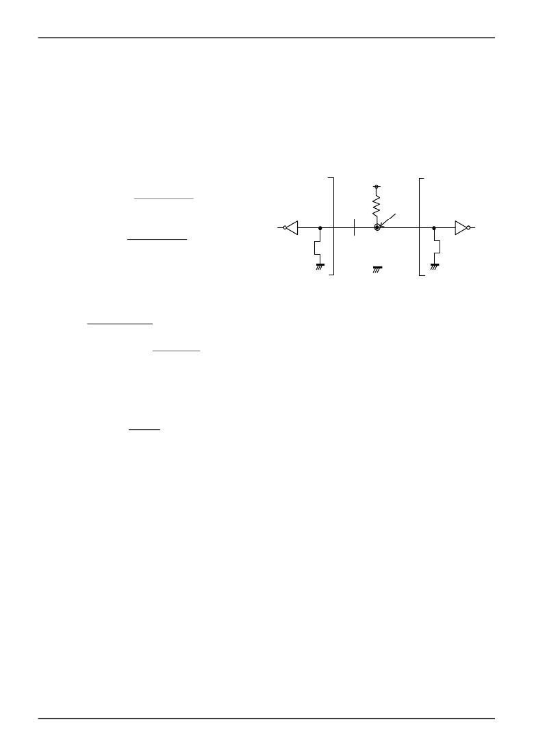
�●� I/O� peripheral� circuit�
�○� Pull� up� resistance� of� SDA� terminal�
�SDA� is� NMOS� open� drain,� so� requires� pull� up� resistance.� As� for� this� resistance� value� (R� PU� ),� select� an� appropriate� value� to�
�this� resistance� value� from� microcontroller� V� IL� ,� I� L� ,� and� V� OL� -I� OL� characteristics� of� this� IC.� If� R� PU� is� large,� action� frequency� is�
�limited.� The� smaller� the� R� PU� ,� the� larger� the� consumption� current� at� action.�
�○� Maximum� value� of� R� PU�
�The� maximum� value� of� R� PU� is� determined� by� the� following� factors.�
�(1)SDA� rise� time� to� be� determined� by� the� capacitance� (CBUS)� of� bus� line� of� R� PU� and� SDA� should� be� tR� or� below.�
�And� AC� timing� should� be� satisfied� even� when� SDA� rise� time� is� late.�
�(2)The� bus� electric� potential� A� to� be� determined� by� input� leak� total� (I� L� )� of� device� connected� to� bus� output� of� 'H'� to� SDA�
�bus� and� R� PU� should� sufficiently� secure� the� input� 'H'� level� (V� IH� )� of� microcontroller� and� EEPROM� including� recommended�
�noise� margin� 0.2Vcc.�
�Vcc� -� I� L� R� PU� -� 0.2Vcc� ≧� V� IH�
�Microcontroller�
�BR24SXX�
�∴�
�R� PU�
�≦�
�0.8V� CC� -� V� IH�
�I� L�
�Ex.)� When� Vcc� =� 3V,� I� L� =10� μ� A,� V� IH� =� 0.7Vcc�
�from(2)�
�10×10�
�R� PU� ≦�
�0.8×3� -� 0.7×3�
�-6�
�≦� 300� [� k� ?� ]�
�○� Minimum� value� of� R� PU�
�The� minimum� value� of� R� PU� is� determined� by� the� following� factors.�
�(1)When� IC� outputs� LOW,� it� should� be� satisfied� that� V� OLMAX� =0.4V�
�and� I� OLMAX� =3mA.�
�Bus� line�
�capacity�
�CBUS�
�Fig.49� I/O� circuit� diagram�
�V� CC� -� V� OL�
�R� PU�
�≦�
�I� OL�
�∴�
�R� PU�
�≧�
�V� CC� -� V� OL�
�I� OL�
�(2)V� OLMAX� =0.4V� should� secure� the� input� 'L'� level� (V� IL� )� of� microcontroller� and� EEPROM� including� recommended� noise� margin� 0.1Vcc.�
�V� OLMAX� ≦� V� IL� -0.1� Vcc�
�Ex.)� When� Vcc=� 3V,� V� OL� 0.4V,� I� OL� =3mA,� microcontroller,� EEPROM� V� IL� =0.3Vcc�
�from(1),�
�R� PU�
�≧�
�3� -� 0.4�
�3×10�
�≧�
�867�
�[� ?� ]�
�And�
�V� OL� =0.4� [� V� ]�
�V� IL� =0.3� � 3�
�=0.9� [� V� ]�
�Therefore,� the� condition� (2)� is� satisfied.�
�○� Pull� up� resistance� of� SCL� terminal�
�When� SCL� control� is� made� at� CMOS� output� port,� there� is� no� need,� but� in� the� case� there� is� timing� where� SCL� becomes�
�'Hi-Z',� add� a� pull� up� resistance.� As� for� the� pull� up� resistance,� one� of� several� k� ?� ~� several� ten� k� ?� is� recommended� in�
�consideration� of� drive� performance� of� output� port� of� microcontroller.�
�●� A0,� A1,� A2,� WP� process�
�○� Process� of� device� address� terminals� (A0,A1,A2)�
�Check� whether� the� set� device� address� coincides� with� device� address� input� sent� from� the� master� side� or� not,� and� select�
�one� among� plural� devices� connected� to� a� same� bus.� Connect� this� terminal� to� pull� up� or� pull� down,� or� Vcc� or� GND.� And,�
�pins(Don't� use� PIN)� not� used� as� device� address� may� be� set� to� any� of� 'H'� ,� 'L',� and� 'Hi-Z'.�
�Types� with� Don't� use� PIN� BR24S08F/FJ/FV/FVT/FVM/FVJ/NUX-W� A0,� A1�
�BR24S16F/FJ/FV/FVT/FVM/FVJ/NUX-W� A0,� A1,� A2�
�○� Process� of� WP� terminal�
�WP� terminal� is� the� terminal� that� prohibits� and� permits� write� in� hardware� manner.� In� 'H'� status,� only� READ� is� available� and�
�WRITE� of� all� address� is� prohibited.� In� the� case� of� 'L',� both� are� available.� In� the� case� of� use� it� as� an� ROM,� it� is�
�recommended� to� connect� it� to� pull� up� or� Vcc.� In� the� case� to� use� both� READ� and� WRITE,� control� WP� terminal� or� connect�
�it� to� pull� down� or� GND.�
�www.rohm.com�
�?� 2009� ROHM� Co.,� Ltd.� All� rights� reserved.�
�34/40�
�2009.09� -� Rev.D�
�相关PDF资料 |
PDF描述 |
|---|---|
| BR24S64FVM-WTR | IC EEPROM 64KBIT 100KHZ MSOP8 |
| BR24S32NUX-WTR | IC EEPROM 32KBIT 100KHZ VSON8 |
| BR25L160F-WE2 | IC EEPROM SER 16KB SPI BUS 8SOP |
| AT24C128C-SSHM-T | IC EEPROM 128KBIT 400KHZ 8SOIC |
| XC6VLX75T-3FFG484C | IC FPGA VIRTEX 6 74K 484FFGBGA |
相关代理商/技术参数 |
参数描述 |
|---|---|
| BR24S64F-WTR | 制造商:ROHM 制造商全称:Rohm 功能描述:High Reliability Series EEPROMs I2C BUS |
| BR24S64NUX-WE2 | 制造商:ROHM 制造商全称:Rohm 功能描述:High Reliability Series EEPROMs I2C BUS |
| BR24S64NUX-WTR | 制造商:ROHM 制造商全称:Rohm 功能描述:High Reliability Series EEPROMs I2C BUS |
| BR24S64-W | 制造商:ROHM 制造商全称:Rohm 功能描述:I2C BUS Serial EEPROMs |
| BR24SXX-W | 制造商:ROHM 制造商全称:Rohm 功能描述:I2C BUS Serial EEPROMs |
发布紧急采购,3分钟左右您将得到回复。